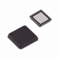
AD8195ACPZ-R7 Analog Devices Inc, AD8195ACPZ-R7 Datasheet - Page 13

AD8195ACPZ-R7
Manufacturer Part Number
AD8195ACPZ-R7
Description
Front Panel HDMI Buffer
Manufacturer
Analog Devices Inc
Datasheet
1.AD8195ACPZ-R7.pdf
(20 pages)
Specifications of AD8195ACPZ-R7
Function
Switch
Circuit
1 x 1:1
Voltage Supply Source
Single Supply
Voltage - Supply, Single/dual (±)
3 V ~ 3.6 V
Current - Supply
40mA
Operating Temperature
-40°C ~ 85°C
Mounting Type
Surface Mount
Package / Case
40-VFQFN, CSP Exposed Pad
Lead Free Status / RoHS Status
Lead free / RoHS Compliant
Available stocks
Company
Part Number
Manufacturer
Quantity
Price
Company:
Part Number:
AD8195ACPZ-R7
Manufacturer:
MITSUBISHI
Quantity:
101
PREEMPHASIS
The preemphasized TMDS outputs precompensate the trans-
mitted signal to account for losses in systems with long cable
runs. These long cable runs selectively attenuate the high
frequency energy of the signal, leading to degraded transition
times and eye closure. Similar to a receive equalizer, the goal of
the preemphasis filter is to boost the high frequency energy in
the signal. However, unlike the receive equalizer, the preemphasis
filter is applied before the channel, thus predistorting the
transmitted signal to account for the loss of the channel. The
series connection of the preemphasis filter and the channel
results in a flatter frequency response than that of the channel,
thus leading to improved high frequency energy, improved
transition times, and improved eye opening on the far end of
the channel. Using a preemphasis filter to compensate for
channel losses allows for longer cable runs with or without a
receiver equalizer on the far end of the channel. In the case that
there is no receive equalizer on the far end of the channel, the
preemphasis filter should allow longer cable runs than would be
acceptable with no preemphasis. In the case of both a preem-
phasis filter on the near end and a receive equalizer on the far
end of the channel, the allowable cable run should be longer
than either compensation could achieve alone. The pulse
response of a preemphasized waveform is shown in Figure 28.
The output voltage levels and symbol descriptions are listed in
Table 9 and Table 10, respectively.
Table 9. Output Voltage Levels
PE Setting
0
1
Table 10. Symbol Definitions
Symbol
V
V
V
V
V
OSE-DC
OSE-BOOST
OCM
H
L
V
V
PREEMPHASIS ON
PREEMPHASIS OFF
V
V
OCM
OCM
TTO
TTO
(DC-Coupled)
<T
Figure 28. Preemphasis Pulse Response
BIT
Boost (dB)
0
6
Formula
I
I
V
V
V
T
T
|
TTO
OCM
OCM
PE = 0
× 25 Ω
I
20
40
– I
T
+ V
− V
(mA)
× 25 Ω
T
/2 × 25 Ω
OSE-BOOST
OSE-BOOST
V
V
OSE-DC
OSE-DC
/2
/2
V
500
500
V
OSE-DC
OSE-BOOST
V
V
(mV p-p)
V
V
H
L
H
L
Rev. 0 | Page 13 of 20
Definition
Boosted single-ended output voltage swing
Single-ended output voltage swing after settling
Common-mode voltage when the output is dc-coupled
High single-ended output voltage excursion
Low single-ended output voltage excursion
AUXILIARY LINES
The auxiliary (low speed) lines provide buffering for the Display
Data Channel (DDC) and Consumer Electronics Control (CEC)
signals. The auxiliary lines are powered independently from the
TMDS link; therefore, their functionality can be maintained even
when the system is powered off. In an application, these lines can
be powered by connecting AMUXVCC to the 5 V supply pro-
vided from the video source through the input HDMI connector.
DDC Buffers
The DDC buffers are 5 V tolerant bidirectional lines that can
carry extended display identification data (EDID), HDCP
encryption, and other information, depending on the specific
application. The DDC buffers are bidirectional and fully support
arbitration, clock synchronization, clock stretching, slave acknowl-
edgement, and other relevant features of a standard mode I
The DDC buffers also have separate voltage references for the
input side and the output side, allowing the sink to use internal
bus voltages (3.3 V), alleviating the need for 5 V tolerant I/Os
for system ASICs. The logic level for the DDC_IN bus is set by
the voltage on VREF_IN, and the logic level for the DDC_OUT
bus is set by the voltage on VREF_OUT. For example, if the
DDC_IN bus is using 5 V I
should be connected to a 5 V power supply. If the DDC_OUT
bus is using 3.3 V I
be connected to a 3.3 V power supply.
CEC Buffer
The CEC buffer is a 3.3 V tolerant bidirectional buffer with
integrated pull-up resistors. This buffer enables full compliance
with all CEC specifications, including but not limited to input
capacitance, logic levels, transition times, and leakage (both
with the system power on and off). This allows the CEC func-
tionality to be implemented in a standard microcontroller that
may not have CEC compliant I/Os. The CEC buffer is powered
from the AMUXVCC supply.
V
500
1000
OSE-BOOST
(mV p-p)
2
C, the VREF_OUT power supply pin should
2
C, the VREF_IN power supply pin
V
3.050
2.8
OCM
(V)
V
3.3
3.3
H
(V)
AD8195
V
2.8
2.3
2
C bus.
L
(V)


