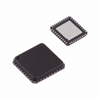
AD8195ACPZ-R7 Analog Devices Inc, AD8195ACPZ-R7 Datasheet - Page 17

AD8195ACPZ-R7
Manufacturer Part Number
AD8195ACPZ-R7
Description
Front Panel HDMI Buffer
Manufacturer
Analog Devices Inc
Datasheet
1.AD8195ACPZ-R7.pdf
(20 pages)
Specifications of AD8195ACPZ-R7
Function
Switch
Circuit
1 x 1:1
Voltage Supply Source
Single Supply
Voltage - Supply, Single/dual (±)
3 V ~ 3.6 V
Current - Supply
40mA
Operating Temperature
-40°C ~ 85°C
Mounting Type
Surface Mount
Package / Case
40-VFQFN, CSP Exposed Pad
Lead Free Status / RoHS Status
Lead free / RoHS Compliant
Available stocks
Company
Part Number
Manufacturer
Quantity
Price
Company:
Part Number:
AD8195ACPZ-R7
Manufacturer:
MITSUBISHI
Quantity:
101
TMDS Terminations
The AD8195 provides internal 50 Ω single-ended terminations
for all of its high speed inputs and outputs. It is not necessary to
include external termination resistors for the TMDS differential
pairs on the PCB.
The output termination resistors of the AD8195 back terminate
the output TMDS transmission lines. These back terminations
act to absorb reflections from impedance discontinuities on the
output traces, improving the signal integrity of the output traces
and adding flexibility to how the output traces can be routed.
For example, interlayer vias can be used to route the AD8195
TMDS outputs on multiple layers of the PCB without severely
degrading the quality of the output signal.
Auxiliary Control Signals
There are three single-ended control signals associated with
each source or sink in an HDMI/DVI application. These are
consumer electronics control (CEC) and two display data
channel (DDC) lines. The two signals on the DDC bus are SDA
and SCL (serial data and serial clock, respectively). These three
signals can be buffered through the AD8195 and do not need to
be routed with the same strict considerations as the high speed
TMDS signals.
In general, it is sufficient to route each auxiliary signal as a
single-ended trace. These signals are not sensitive to impedance
discontinuities, do not require a reference plane, and can be
routed on multiple layers of the PCB. However, it is best to
follow strict layout practices whenever possible to prevent the
PCB design from affecting the overall application. The specific
routing of the CEC and DDC lines depends on the application
in which the AD8195 is being used.
For example, the maximum speed of signals present on the
auxiliary lines is 100 kHz I
any layout that enables 100 kHz I
bus should suffice. The HDMI 1.3a specification, however,
places a strict 50 pF limit on the amount of capacitance that can
be measured on either SDA or SCL at the HDMI input connector.
This 50 pF limit includes the HDMI connector, the PCB, and
whatever capacitance is seen at the input of the AD8195. There
is a similar limit of 150 pF of input capacitance for the CEC line.
The parasitic capacitance of traces on a PCB increases with
trace length. To help ensure that a design satisfies the HDMI
specification, the length of the CEC and DDC lines on the PCB
should be made as short as possible. Additionally, if there is a
reference plane in the layer adjacent to the auxiliary traces in
the PCB stack-up, relieving or clearing out this reference plane
immediately under the auxiliary traces significantly decreases
the amount of parasitic trace capacitance. An example of the
board stack-up is shown in Figure 31.
2
C data on the DDC lines; therefore,
2
C to be passed over the DDC
Rev. 0 | Page 17 of 20
The AD8195 buffers the auxiliary signals; therefore, only the
input traces, connector, and AD8195 input capacitance must be
considered when designing a PCB to meet HDMI specifications.
Power Supplies
The AD8195 has four separate power supplies referenced to a
single ground, AVEE. The supply/ground pairs are
•
•
•
•
The AVCC/AVEE (3.3 V) supply powers the core of the AD8195.
The VTTI/AVEE supply (3.3 V) powers the input termination
(see Figure 26). Similarly, the VTTO/AVEE supply (3.3 V)
powers the output termination (see Figure 27). The AMUXVCC/
AVEE supply (5 V) powers the auxiliary buffer core.
In a typical application, all pins labeled AVEE should be connected
directly to ground. All pins labeled AVCC, VTTI, or VTTO
should be connected to 3.3 V, and Pin AMUXVCC should be
tied to 5 V. The AVCC supply powers the TMDS buffers while
AMUXVCC powers the DDC/CEC buffers. AMUXVCC can be
connected to the +5 V supply provided from the input HDMI
connector to ensure that the DDC and CEC buffers remain
functional when the system is powered off. The supplies can
also be powered individually, but care must be taken to ensure
that each stage of the AD8195 is powered correctly.
DDC Reference Inputs
The VREF_IN and VREF_OUT voltages (3.3 V to 5 V) provide
reference levels for the DDC buffers. Both voltages are
referenced to AVEE. The voltage applied at these reference
inputs should be the same as the pull-up voltage for
corresponding DDC bus.
AVCC/AVEE
VTTI/AVEE
VTTO/AVEE
AMUXVCC/AVEE.
SILKSCREEN
LAYER 1: MICROSTRIP
PCB DIELECTRIC
LAYER 2: REFERENCE PLANE
PCB DIELECTRIC
LAYER 3: REFERENCE PLANE
PCB DIELECTRIC
LAYER 4: MICROSTRIP
SILKSCREEN
Figure 31. Example Board Stack-Up
3W
RELIEVED UNDERNEATH
REFERENCE LAYER
MICROSTRIP
W
3W
AD8195


