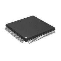
AD8197ASTZ-RL Analog Devices Inc, AD8197ASTZ-RL Datasheet - Page 15

AD8197ASTZ-RL
Manufacturer Part Number
AD8197ASTZ-RL
Description
IC,Telecom Switching Circuit,QFP,100PIN,PLASTIC
Manufacturer
Analog Devices Inc
Datasheet
1.AD8197ASTZ-RL.pdf
(32 pages)
Specifications of AD8197ASTZ-RL
Function
Switch
Circuit
1 x 4:1
On-state Resistance
50 Ohm
Voltage Supply Source
Single Supply
Voltage - Supply, Single/dual (±)
3 V ~ 3.6 V
Current - Supply
40mA
Operating Temperature
-40°C ~ 85°C
Mounting Type
Surface Mount
Package / Case
100-LQFP
Lead Free Status / RoHS Status
Lead free / RoHS Compliant
Available stocks
Company
Part Number
Manufacturer
Quantity
Price
Company:
Part Number:
AD8197ASTZ-RL
Manufacturer:
Analog Devices Inc
Quantity:
10 000
This precaution does not need to be taken if the DDC
peripheral circuitry is connected to the bus downstream of
the AD8197.
AUXILIARY (LOW SPEED) SWITCHING MODES
The AD8197 has three auxiliary switching modes: quad, dual,
and single. These are selected by programming the AUX_SM
bits of the auxiliary device modes register through the serial
control interface. The auxiliary switching mode is independent
of the high speed switching mode whenever the part is controlled
through the serial control interface. When the part is controlled
through the parallel control interface, however, only quad mode
is accessible and the auxiliary switching mode cannot be
independently controlled.
SOURCE A +5V
SOURCE B +5V
PIN 18 HDMI CONNECTOR
PIN 18 HDMI CONNECTOR
PIN 14 DVI CONNECTOR
PIN 14 DVI CONNECTOR
PERIPHERAL
PERIPHERAL
Figure 28. Suggested AMUXVCC Power Scheme
CIRCUITRY
CIRCUITRY
|<50mA
|<50mA
10kΩ
10kΩ
+5V INTERNAL
10MΩ
AMUXVCC
AD8197
(IF ANY)
PIN 18 HDMI CONNECTOR
PIN 18 HDMI CONNECTOR
PIN 14 DVI CONNECTOR
PIN 14 DVI CONNECTOR
|<50mA
|<50mA
10kΩ
10kΩ
PERIPHERAL
PERIPHERAL
CIRCUITRY
CIRCUITRY
+5V SOURCE C
+5V SOURCE D
Rev. 0 | Page 15 of 32
Quad Switching Mode
This is the default mode. In quad mode, the AD8197 behaves
like a 4:1 auxiliary link multiplexer, routing groups of four
auxiliary input signals to the four-signal output. Select which
group of inputs is routed to the output by programming the
AUX_CH bits of the auxiliary device modes register through
the serial control interface in accordance with the switch
mapping listed in Table 13. Alternately, select which group of
inputs is routed to the output by setting the PP_CH bus of the
parallel control interface in accordance with the switch
mapping listed in Table 27.
Dual Switching Mode
In this mode, the AD8197 behaves as a locked dual [8:1]
auxiliary signal switch. The two 8:1 switches share the channel
select input and, therefore, switch together. Select which two
out of the eight possible input groups are routed to the output
by programming the AUX_CH bits of the auxiliary device
modes register in accordance with the switch mapping listed in
Table 14. This mode is only accessible through the serial control
interface.
Single Switching Mode
In this mode the AD8197 behaves as a single 16:1 TMDS
channel multiplexer; a single channel, out of a possible 16,
is routed to all of the outputs. Select which input channel is
routed to the outputs by programming the AUX_CH bits of the
auxiliary device modes register in accordance with the switch
mapping listed in Table 15. This mode is only accessible
through the serial control interface.
AD8197


