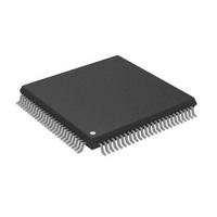
AD8197ASTZ-RL Analog Devices Inc, AD8197ASTZ-RL Datasheet - Page 19

AD8197ASTZ-RL
Manufacturer Part Number
AD8197ASTZ-RL
Description
IC,Telecom Switching Circuit,QFP,100PIN,PLASTIC
Manufacturer
Analog Devices Inc
Datasheet
1.AD8197ASTZ-RL.pdf
(32 pages)
Specifications of AD8197ASTZ-RL
Function
Switch
Circuit
1 x 4:1
On-state Resistance
50 Ohm
Voltage Supply Source
Single Supply
Voltage - Supply, Single/dual (±)
3 V ~ 3.6 V
Current - Supply
40mA
Operating Temperature
-40°C ~ 85°C
Mounting Type
Surface Mount
Package / Case
100-LQFP
Lead Free Status / RoHS Status
Lead free / RoHS Compliant
Available stocks
Company
Part Number
Manufacturer
Quantity
Price
Company:
Part Number:
AD8197ASTZ-RL
Manufacturer:
Analog Devices Inc
Quantity:
10 000
SERIAL INTERFACE CONFIGURATION REGISTERS
The serial interface configuration registers can be read and written using the I
The least significant bits of the AD8197 I
3.3 V (Logic 1) or 0 V (Logic 0). As soon as the serial control interface is used, the parallel control interface is disabled until the AD8197
is reset as described in the Serial Control Interface section.
Table 5. Serial (I
Name
High Speed
Device
Modes
Auxiliary
Device
Modes
Receiver
Settings
Input
Termination
Pulse 1
Input
Termination
Pulse 2
Receive
Equalizer 1
Receive
Equalizer 2
Transmitter
Settings
HIGH SPEED DEVICE MODES REGISTER
HS_EN: High Speed (TMDS) Channels Enable Bit
Table 6. HS_EN Description
HS_EN
0
1
HS_SM[1:0]: High Speed (TMDS) Switching Mode
Select Bus
Table 7. HS_SM Description
HS_SM[1:0]
00
01
10
11
Description
High speed channels off, low power/standby mode
High speed channels on
Bit 7
RX_PT[15]
RX_EQ[15]
RX_EQ[7]
RX_PT[7]
2
C) Interface Register Map
Description
Quad mode, 4× [4:1]
Dual mode, 2× [8:1]
Single mode, 1× [16:1]
Illegal value; previous value of HS_SM[1:0]
retained
Bit 6
High
speed
switch
enable
HS_EN
Auxiliary
switch
enable
AUX_EN
RX_PT[6]
RX_PT[14]
RX_EQ[6]
RX_EQ[14]
Source A and Source B : input termination pulse-on-source switch select
Source C and Source D: input termination pulse-on-source switch select
Bit 5
HS_SM[1]
AUX_SM[1]
RX_PT[5]
RX_PT[13]
RX_EQ[5]
RX_EQ[13]
2
C part address are set by tying the Pin I2C_ADDR2, Pin I2C_ADDR1, and Pin I2C_ADDR0 to
Source A and Source B: input equalization level select
Source C and Source D: input equalization level select
High speed switching
Auxiliary switching
(disconnect termination for a short period of time)
(disconnect termination for a short period of time)
mode select
mode select
Bit 4
HS_SM[0]
AUX_SM[0]
RX_PT[4]
RX_PT[12]
RX_EQ[4]
RX_EQ[12]
Rev. 0 | Page 19 of 32
Bit 3
HS_CH[3]
AUX_CH[3]
RX_PT[3]
RX_PT[11]
RX_EQ[3]
RX_EQ[11]
TX_PE[1]
pre-emphasis level select
High speed output
HS_CH[3:0]: High Speed (TMDS) Switch Source Select Bus
Table 8. Quad Mode, 4× [4:1], High Speed Switch Mapping
HS_CH[3:0]
XX00
XX01
XX10
XX11
2
C serial control interface, Pin I2C_SDA, and Pin I2C_SCL.
Auxiliary switch source select
Bit 2
HS_CH[2]
AUX_CH[2]
RX_PT[2]
RX_PT[10]
RX_EQ[2]
RX_EQ[10]
TX_PE[0]
High speed source select
O[3:0]
A[3:0]
B[3:0]
C[3:0]
D[3:0]
Bit 1
HS_CH[1]
AUX_CH[1]
RX_PT[1]
RX_PT[9]
RX_EQ[1]
RX_EQ[9]
High speed
output
termination
select
TX_PTO
Description
High Speed Source A switched to
output
High Speed Source B switched to
output
High Speed Source C switched to
output
High Speed Source D switched to
output
Bit 0
HS_CH[0]
AUX_CH[0]
High speed
input
termination
select
RX_TO
RX_PT[0]
RX_PT[8]
RX_EQ[0]
RX_EQ[8]
High speed
output
current
level select
TX_OCL
Addr.
0x00
0x01
0x10
0x11
0x12
0x13
0x14
0x20
AD8197
Default
0x40
0x40
0x01
0x00
0x00
0x00
0x00
0x03


