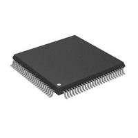
AD8197ASTZ-RL Analog Devices Inc, AD8197ASTZ-RL Datasheet - Page 27

AD8197ASTZ-RL
Manufacturer Part Number
AD8197ASTZ-RL
Description
IC,Telecom Switching Circuit,QFP,100PIN,PLASTIC
Manufacturer
Analog Devices Inc
Datasheet
1.AD8197ASTZ-RL.pdf
(32 pages)
Specifications of AD8197ASTZ-RL
Function
Switch
Circuit
1 x 4:1
On-state Resistance
50 Ohm
Voltage Supply Source
Single Supply
Voltage - Supply, Single/dual (±)
3 V ~ 3.6 V
Current - Supply
40mA
Operating Temperature
-40°C ~ 85°C
Mounting Type
Surface Mount
Package / Case
100-LQFP
Lead Free Status / RoHS Status
Lead free / RoHS Compliant
Available stocks
Company
Part Number
Manufacturer
Quantity
Price
Company:
Part Number:
AD8197ASTZ-RL
Manufacturer:
Analog Devices Inc
Quantity:
10 000
interference, route the TMDS signals away from other signals
and noise sources on the PCB.
Both traces of a given differential pair must be equal in length
to minimize intrapair skew. Maintaining the physical symmetry
of a differential pair is integral to ensuring its signal integrity;
excessive intrapair skew can introduce jitter through duty cycle
distortion (DCD). The p and n of a given differential pair should
always be routed together to establish the required 100 Ω differ-
ential impedance. Enough space should be left between the
differential pairs of a given group so that the n of one pair does
not couple to the p of another pair. For example, one technique is
to make the interpair distance 4 to 10 times wider than the
intrapair spacing.
Any group of four TMDS channels (Input A, Input B, Input C,
Input D, or the output) should have closely matched trace
lengths to minimize interpair skew. Severe interpair skew can
cause the data on the four different channels of a group to arrive
out of alignment with one another. A good practice is to match
the trace lengths for a given group of four channels to within
0.05 inches on FR4 material.
Minimizing intrapair and interpair skew becomes increasingly
important as data rates increase. Any introduced skew will
constitute a correspondingly larger fraction of a bit period at
higher data rates.
Though the AD8197 features input equalization and output pre-
emphasis, the length of the TMDS traces should be minimized
to reduce overall signal degradation. Commonly used PC board
material such as FR4 is lossy at high frequencies; therefore, long
traces on the circuit board increase signal attenuation resulting
in decreased signal swing and increased jitter through
intersymbol interference (ISI).
Controlling the Characteristic Impedance of a TMDS
Differential Pair
The characteristic impedance of a differential pair depends
on a number of variables, including the trace width, the
distance between the two traces, the height of the dielectric
material between the trace and the reference plane below it,
and the dielectric constant of the PCB binder material. To
a lesser extent, the characteristic impedance also depends
upon the trace thickness and the presence of solder mask.
There are many combinations that can produce the correct
characteristic impedance. Generally, working with the PC board
fabricator is required to obtain a set of parameters to produce
the desired results.
One consideration is how to guarantee a differential pair with
a differential impedance of 100 Ω over the entire length of the
trace. One technique to accomplish this is to change the width
of the traces in a differential pair based on how closely one trace
is coupled to the other. When the two traces of a differential
pair are close and strongly coupled, they should have a width
that produces a 100 Ω differential impedance. When the traces
split apart, to go into a connector, for example, and are no
Rev. 0 | Page 27 of 32
longer so strongly coupled, the width of the traces should be
increased to yield a differential impedance of 100 Ω in the new
configuration.
Ground Current Return
In some applications, it can be necessary to invert the output
pin order of the AD8197. This requires a designer to route the
TMDS traces on multiple layers of the PCB. When routing
differential pairs on multiple layers, it is also necessary to
reroute the corresponding reference plane in order to provide
one continuous ground current return path for the differential
signals. Standard plated through-hole vias are acceptable for
both the TMDS traces and the reference plane. An example of
this is illustrated in Figure 32.
TMDS Terminations
The AD8197 provides internal, 50 Ω single-ended terminations
for all of its high speed inputs and outputs. It is not necessary to
include external termination resistors for the TMDS differential
pairs on the PCB.
The output termination resistors of the AD8197 back-terminate
the output TMDS transmission lines. These back-terminations
act to absorb reflections from impedance discontinuities on the
output traces, improving the signal integrity of the output traces
and adding flexibility to how the output traces can be routed.
For example, interlayer vias can be used to route the AD8197
TMDS outputs on multiple layers of the PCB without severely
degrading the quality of the output signal.
Auxiliary Control Signals
There are four single-ended control signals associated with each
source or sink in an HDMI/DVI application. These are hot plug
detect (HPD), consumer electronics control (CEC), and two
display data channel (DDC) lines. The two signals on the DDC
bus are SDA and SCL (serial data and serial clock, respectively).
These four signals can be switched through the auxiliary bus of
SILKSCREEN
LAYER 1: SIGNAL (MICROSTRIP)
PCB DIELECTRIC
LAYER 2: GND (REFERENCE PLANE)
PCB DIELECTRIC
LAYER 3: PWR
(REFERENCE PLANE)
PCB DIELECTRIC
LAYER 4: SIGNAL (MICROSTRIP)
SILKSCREEN
Figure 32. Example Routing of Reference Plane
KEEP REFERENCE PLANE
ADJACENT TO SIGNAL ON ALL
LAYERS TO PROVIDE CONTINUOUS
GROUND CURRENT RETURN PATH.
THROUGH-HOLE VIAS
AD8197


