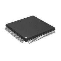
AD8197ASTZ-RL Analog Devices Inc, AD8197ASTZ-RL Datasheet - Page 28

AD8197ASTZ-RL
Manufacturer Part Number
AD8197ASTZ-RL
Description
IC,Telecom Switching Circuit,QFP,100PIN,PLASTIC
Manufacturer
Analog Devices Inc
Datasheet
1.AD8197ASTZ-RL.pdf
(32 pages)
Specifications of AD8197ASTZ-RL
Function
Switch
Circuit
1 x 4:1
On-state Resistance
50 Ohm
Voltage Supply Source
Single Supply
Voltage - Supply, Single/dual (±)
3 V ~ 3.6 V
Current - Supply
40mA
Operating Temperature
-40°C ~ 85°C
Mounting Type
Surface Mount
Package / Case
100-LQFP
Lead Free Status / RoHS Status
Lead free / RoHS Compliant
Available stocks
Company
Part Number
Manufacturer
Quantity
Price
Company:
Part Number:
AD8197ASTZ-RL
Manufacturer:
Analog Devices Inc
Quantity:
10 000
AD8197
the AD8197 and do not need to be routed with the same strict
considerations as the high speed TMDS signals.
In general, it is sufficient to route each auxiliary signal as a
single-ended trace. These signals are not sensitive to impedance
discontinuities, do not require a reference plane, and can be
routed on multiple layers of the PCB. However, it is best to
follow strict layout practices whenever possible to prevent the
PCB design from affecting the overall application. The specific
routing of the HPD, CEC, and DDC lines depends upon the
application in which the AD8197 is being used.
For example, the maximum speed of signals present on the
auxiliary lines is 100 kHz I
any layout that enables 100 kHz I
bus should suffice. The HDMI 1.3 specification, however, places
a strict 50 pF limit on the amount of capacitance that can be
measured on either SDA or SCL at the HDMI input connector.
This 50 pF limit includes the HDMI connector, the PCB, and
whatever capacitance is seen at the input of the AD8197, or an
equivalent receiver. There is a similar limit of 100 pF of input
capacitance for the CEC line.
The parasitic capacitance of traces on a PCB increases with
trace length. To help ensure that a design satisfies the HDMI
specification, the length of the CEC and DDC lines on the PCB
should be made as short as possible. Additionally, if there is a
reference plane in the layer adjacent to the auxiliary traces in
the PCB stack-up, relieving or clearing out this reference plane
immediately under the auxiliary traces significantly decreases
the amount of parasitic trace capacitance. An example of the
board stackup is shown in Figure 33.
SILKSCREEN
LAYER 1: SIGNAL (MICROSTRIP)
PCB DIELECTRIC
LAYER 2: GND (REFERENCE PLANE)
PCB DIELECTRIC
LAYER 3: PWR (REFERENCE PLANE)
PCB DIELECTRIC
LAYER 4: SIGNAL (MICROSTRIP)
SILKSCREEN
Figure 33. Example Board Stackup
2
C data on the DDC lines; therefore,
2
C to be passed over the DDC
3W
RELIEVED UNDERNEATH
REFERENCE LAYER
MICROSTRIP
W
3W
Rev. 0 | Page 28 of 32
HPD is a dc signal presented by a sink to a source to indicate
that the source EDID is available for reading. The placement
of this signal is not critical, but it should be routed as directly
as possible.
When the AD8197 is powered up, one set of the auxiliary in-
puts is passively routed to the outputs. In this state, the AD8197
looks like a 100 Ω resistor between the selected auxiliary inputs
and the corresponding outputs as illustrated in Figure 27. The
AD8197 does not buffer the auxiliary signals, therefore, the
input traces, output traces, and the connection through the
AD8197 all must be considered when designing a PCB to meet
HDMI/DVI specifications. The unselected auxiliary inputs of the
AD8197 are placed into a high impedance mode when the device
is powered up. To ensure that all of the auxiliary inputs of the
AD8197 are in a high impedance mode when the device is powered
off, it is necessary to power the AMUXVCC supply as illustrated
in Figure 28.
In contrast to the auxiliary signals, the AD8197 buffers the
TMDS signals, allowing a PCB designer to layout the TMDS
inputs independently of the outputs.
Power Supplies
The AD8197 has five separate power supplies referenced to
two separate grounds. The supply/ground pairs are:
•
•
•
•
•
The AVCC/AVEE (3.3 V) and DVCC/DVEE (3.3 V) supplies
power the core of the AD8197. The VTTI/AVEE supply (3.3 V)
powers the input termination (see Figure 25). Similarly, the
VTTO/AVEE supply (3.3 V) powers the output termination
(see Figure 26). The AMUXVCC/DVEE supply (3.3 V to 5 V)
powers the auxiliary multiplexer core and determines the
maximum allowed voltage on the auxiliary lines. For example,
if the DDC bus is using 5 V I
connected to +5 V relative to DVEE.
In a typical application, all pins labeled AVEE or DVEE should
be connected directly to ground. All pins labeled AVCC,
DVCC, VTTI, or VTTO should be connected to 3.3 V, and
Pin AMUXVCC tied to 5 V. The supplies can also be powered
individually, but care must be taken to ensure that each stage of
the AD8197 is powered correctly.
AVCC/AVEE
VTTI/AVEE
VTTO/AVEE
DVCC/DVEE
AMUXVCC/DVEE
2
C, then AMUXVCC should be


