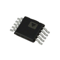
ADP1873ARMZ-0.3-R7 Analog Devices Inc, ADP1873ARMZ-0.3-R7 Datasheet - Page 19

ADP1873ARMZ-0.3-R7
Manufacturer Part Number
ADP1873ARMZ-0.3-R7
Description
300kHz, Light Load Eff Enabled
Manufacturer
Analog Devices Inc
Datasheet
1.ADP1872ARMZ-0.6-R7.pdf
(40 pages)
Specifications of ADP1873ARMZ-0.3-R7
Pwm Type
Current Mode
Number Of Outputs
1
Frequency - Max
300kHz
Duty Cycle
84%
Voltage - Supply
2.75 V ~ 20 V
Buck
Yes
Boost
No
Flyback
No
Inverting
No
Doubler
No
Divider
No
Cuk
No
Isolated
No
Operating Temperature
-40°C ~ 125°C
Package / Case
10-MSOP, Micro10™, 10-uMAX, 10-uSOP
Frequency-max
300kHz
Lead Free Status / RoHS Status
Lead free / RoHS Compliant
Other names
ADP1873ARMZ-0.3-R7TR
Available stocks
Company
Part Number
Manufacturer
Quantity
Price
Company:
Part Number:
ADP1873ARMZ-0.3-R7
Manufacturer:
Analog Devices Inc
Quantity:
1 900
PROGRAMMING RESISTOR (RES) DETECT CIRCUIT
Upon startup, one of the first blocks to become active is the RES
detect circuit. This block powers up before soft start begins. It
forces a 0.4 V reference value at the DRVL output (see Figure 67)
and is programmed to identify four possible resistor values: 47 kΩ,
22 kΩ, open, and 100 kΩ.
The RES detect circuit digitizes the value of the resistor at the
DRVL pin (Pin 6). An internal ADC outputs a 2-bit digital code
that is used to program four separate gain configurations in the
current-sense amplifier (see Figure 68). Each configuration
corresponds to a current-sense gain (A
24 V/V, respectively (see Table 5 and Table 6). This variable is used
for the valley current-limit setting, which sets up the appropriate
current-sense gain for a given application and sets the compensation
necessary to achieve loop stability (see the Valley Current-Limit
Setting and Compensation Network sections).
Table 5. Current-Sense Gain Programming
Resistor
47 kΩ
22 kΩ
Open
100 kΩ
Figure 68. RES Detect Circuit for Current-Sense Gain Programming
CS GAIN SET
Figure 67. Programming Resistor Location
DRVL
AMP
CS
PROGRAMMING
RES
ADP1872
ADC
CS GAIN
DRVH
DRVL
SW
A
3
6
12
24
CS
R
(V/V)
RES
CS
0.4V
) of 3 V/V, 6 V/V, 12 V/V,
Q1
Q2
SW
PGND
Rev. A | Page 19 of 40
VALLEY CURRENT-LIMIT SETTING
The architecture of the ADP1872/ADP1873 is based on valley
current-mode control. The current limit is determined by three
components: the R
output voltage swing (COMP), and the current-sense gain. The
COMP range is internally fixed at 1.4 V. The current-sense gain
is programmable via an external resistor at the DRVL pin (see
the Programming Resistor (RES) Detect Circuit section). The R
of the lower side MOSFET can vary over temperature and usually
has a positive T
therefore, it is recommended to program the current-sense gain
resistor based on the rated R
Because the ADP1872/ADP1873 are based on valley current
control, the relationship between I
where:
I
I
K
desired average load current (see Figure 10). Establishing K
helps to determine the inductor value (see the Inductor
Selection section), but in most cases, K
When the desired valley current limit (I
the current-sense gain can be calculated by
where:
A
R
Although the ADP1872/ADP1873 have only four discrete current-
sense gain settings for a given R
outline several available options for the valley current setpoint
based on various R
CLIM
LOAD
ON
I
CS
is the ratio between the inductor ripple current and the
is the current-sense gain multiplier (see Table 5 and Table 6).
is the channel impedance of the lower side MOSFET.
is the desired valley current limit.
is the current load.
I
I
CLIM
CLIM
Figure 69. Valley Current Limit to Average Current Relation
=
=
I
A
LOAD
CS
C
1
LOAD CURRENT
4 .
(meaning that it increases with temperature);
ON
×
VALLEY CURRENT LIMIT
×
ON
V
R
of the lower side MOSFET, the error amplifier
⎛ −
⎜
⎝
ON
1
values.
K
2
I
ON
⎞
⎟
⎠
ON
of the MOSFET at 125°C.
RIPPLE CURRENT =
variable, Table 6 and Figure 70
ADP1872/ADP1873
CLIM
CLIM
and I
I
= 0.33.
) has been determined,
LOAD
I
LOAD
is
3
I
ON


