ADP1873ARMZ-0.3-R7 Analog Devices Inc, ADP1873ARMZ-0.3-R7 Datasheet - Page 6
ADP1873ARMZ-0.3-R7
Manufacturer Part Number
ADP1873ARMZ-0.3-R7
Description
300kHz, Light Load Eff Enabled
Manufacturer
Analog Devices Inc
Datasheet
1.ADP1872ARMZ-0.6-R7.pdf
(40 pages)
Specifications of ADP1873ARMZ-0.3-R7
Pwm Type
Current Mode
Number Of Outputs
1
Frequency - Max
300kHz
Duty Cycle
84%
Voltage - Supply
2.75 V ~ 20 V
Buck
Yes
Boost
No
Flyback
No
Inverting
No
Doubler
No
Divider
No
Cuk
No
Isolated
No
Operating Temperature
-40°C ~ 125°C
Package / Case
10-MSOP, Micro10™, 10-uMAX, 10-uSOP
Frequency-max
300kHz
Lead Free Status / RoHS Status
Lead free / RoHS Compliant
Other names
ADP1873ARMZ-0.3-R7TR
Available stocks
Company
Part Number
Manufacturer
Quantity
Price
Company:

Part Number:
ADP1873ARMZ-0.3-R7
Manufacturer:
Analog Devices Inc
Quantity:
1 900


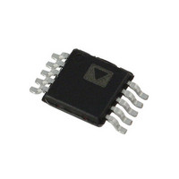
ADP1872/ADP1873
PIN CONFIGURATION AND FUNCTION DESCRIPTIONS
Table 4. Pin Function Descriptions
Pin No.
1
2
3
4
5
6
7
8
9
10
Mnemonic
VIN
COMP/EN
FB
GND
VDD
DRVL
PGND
DRVH
SW
BST
High Input Voltage. Connect VIN to the drain of the upper-side MOSFET.
Output of the Internal Error Amplifier/IC Enable. When this pin functions as EN, applying 0 V to this pin disables the IC.
Analog Ground Reference Pin of the IC. All sensitive analog components should be connected to this ground
plane (see the Layout Considerations Section).
Bias Voltage Supply for the ADP1872/ADP1873 Controller (Includes the Output Gate Drivers). A bypass capacitor
of 1 μF directly from this pin to PGND and a 0.1 μF across VDD and GND are recommended.
Drive Output for the External Lower Side, N-Channel MOSFET. This pin also serves as the current-sense gain
setting pin (see Figure 68).
Power GND. Ground for the lower side gate driver and lower side, N-channel MOSFET.
Switch Node Connection.
Bootstrap for the Upper Side MOSFET Gate Drive Circuitry. An internal boot rectifier (diode) is connected
between VDD and BST. A capacitor from BST to SW is required. An external Schottky diode can also be
connected between VDD and BST for increased gate drive capability.
Description
Noninverting Input of the Internal Error Amplifier. This is the node where the feedback resistor is connected.
Drive Output for the External Upper Side, N-Channel MOSFET.
COMP/EN
GND
VDD
VIN
FB
Figure 3. Pin Configuration
Rev. A | Page 6 of 40
1
2
3
4
5
(Not to Scale)
ADP1872
TOP VIEW
10
9
8
7
6
BST
SW
DRVH
PGND
DRVL
Related parts for ADP1873ARMZ-0.3-R7
Image
Part Number
Description
Manufacturer
Datasheet
Request
R

Part Number:
Description:
600kHz, Light Load Eff Enabled
Manufacturer:
Analog Devices Inc
Datasheet:
Part Number:
Description:
1.0MHz, Light Load Eff Enabled
Manufacturer:
Analog Devices Inc
Datasheet:

Part Number:
Description:
±1.7g Dual-Axis IMEMS Accelerometer Evaluation Board
Manufacturer:
Analog Devices Inc
Datasheet:
Part Number:
Description:
Inertial Sensor Evaluation System
Manufacturer:
Analog Devices Inc
Datasheet:
Part Number:
Description:
Manufacturer:
Analog Devices Inc
Datasheet:
Part Number:
Description:
Manufacturer:
Analog Devices Inc
Datasheet:
Part Number:
Description:
Manufacturer:
Analog Devices Inc
Datasheet:
Part Number:
Description:
Manufacturer:
Analog Devices Inc
Datasheet:
Part Number:
Description:
Manufacturer:
Analog Devices Inc
Datasheet:
Part Number:
Description:
Manufacturer:
Analog Devices Inc
Datasheet:
Part Number:
Description:
Manufacturer:
Analog Devices Inc
Datasheet:
Part Number:
Description:
Manufacturer:
Analog Devices Inc
Datasheet:
Part Number:
Description:
Manufacturer:
Analog Devices Inc
Datasheet: