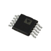
ADP1873ARMZ-0.3-R7 Analog Devices Inc, ADP1873ARMZ-0.3-R7 Datasheet - Page 24

ADP1873ARMZ-0.3-R7
Manufacturer Part Number
ADP1873ARMZ-0.3-R7
Description
300kHz, Light Load Eff Enabled
Manufacturer
Analog Devices Inc
Datasheet
1.ADP1872ARMZ-0.6-R7.pdf
(40 pages)
Specifications of ADP1873ARMZ-0.3-R7
Pwm Type
Current Mode
Number Of Outputs
1
Frequency - Max
300kHz
Duty Cycle
84%
Voltage - Supply
2.75 V ~ 20 V
Buck
Yes
Boost
No
Flyback
No
Inverting
No
Doubler
No
Divider
No
Cuk
No
Isolated
No
Operating Temperature
-40°C ~ 125°C
Package / Case
10-MSOP, Micro10™, 10-uMAX, 10-uSOP
Frequency-max
300kHz
Lead Free Status / RoHS Status
Lead free / RoHS Compliant
Other names
ADP1873ARMZ-0.3-R7TR
Available stocks
Company
Part Number
Manufacturer
Quantity
Price
Company:
Part Number:
ADP1873ARMZ-0.3-R7
Manufacturer:
Analog Devices Inc
Quantity:
1 900
ADP1872/ADP1873
Ceramic capacitors are known to have low ESR. However, the
trade-off of using X5R technology is that up to 80% of its capaci-
tance may be lost due to derating because the voltage applied
across the capacitor is increased (see Figure 79). Although X7R
series capacitors can also be used, the available selection is
limited to only up to 22 μF.
Electrolytic capacitors satisfy the bulk capacitance requirements
for most high current applications. Because the ESR of electrolytic
capacitors is much higher than that of ceramic capacitors, when
using electrolytic capacitors, several MLCCs should be mounted
in parallel to reduce the overall series resistance.
COMPENSATION NETWORK
Due to its current-mode architecture, the ADP1872/ADP1873
require Type II compensation. To determine the component
values needed for compensation (resistance and capacitance
values), it is necessary to examine the converter’s overall loop
gain (H) at the unity gain frequency (f
Examining each variable at high frequency enables the unity
gain transfer function to be simplified to provide expressions
for the R
Output Filter Impedance (Z
Examining the filter’s transfer function at high frequencies
simplifies to
at the crossover frequency (s = 2πf
Figure 79. Capacitance vs. DC Voltage Characteristics for Ceramic Capacitors
–100
H
Z
–10
–20
–30
–40
–50
–60
–70
–80
–90
20
10
FILTER
0
= V/V
COMP
0
1
10µF TDK 25V, X7R, 1210 C3225X7R1E106M
22µF MURATA 25V, X7R, 1210 GRM32ER71E226KE15L
47µF MURATA 16V, X5R, 1210 GRM32ER61C476KE15L
=
and C
sC
=
5
G
1
OUT
COMP
M
X5R (16V)
×
G
component values.
10
CS
DC VOLTAGE (V
×
X7R (50V)
V
X5R (25V)
V
FILT
OUT
REF
15
)
CROSS
×
Z
SW
DC
).
COMP
)
/10) when H = 1 V/V.
20
×
Z
FILT
25
30
Rev. A | Page 24 of 40
Error Amplifier Output Impedance (Z
Assuming C
omitted from the output impedance equation of the error amplifier.
The transfer function simplifies to
and
where f
frequency for the ADP1872.
Error Amplifier Gain (G
The error amplifier gain (transconductance) is
Current-Sense Loop Gain (G
The current-sense loop gain is
where:
A
(see the Programming Resistor (RES) Detect Circuit and Valley
Current-Limit Setting sections).
R
Crossover Frequency
The crossover frequency is the frequency at which the overall
loop (system) gain is 0 dB (H = 1 V/V). It is recommended for
current-mode converters, such as the ADP1872, that the user
set the crossover frequency between 1/10
switching frequency.
The relationship between C
The zero frequency is set to 1/4
Combining all of the above parameters results in
CS
ON
(V/V) is programmable for 3 V/V, 6 V/V, 12 V/V, and 24 V/V
is the channel impedance of the lower side MOSFET.
G
G
C
Z
R
f
f
f
CROSS
CROSS
ZERO
M
COMP
COMP
COMP
CS
ZERO
= 500 μA/V
=
, the zero frequency, is set to be 1/4
=
=
=
=
A
=
=
C2
12
π 2
CS
1
12
R
2
1
is significantly smaller than C
f
CROSS
COMP
×
×
×
1
×
f
π
f
R
SW
R
SW
f
CROSS
×
ON
COMP
(
+
R
f
f
CROSS
1
COMP
CROSS
f
(A/V)
ZERO
1
×
C
M
+
×
COMP
COMP
)
×
f
f
ZERO
ZERO
π 2
th
CS
and f
f
of the crossover frequency.
G
)
CROSS
)
M
G
ZERO
C
CS
OUT
th
(zero frequency) is
COMP
and 1/15
×
COMP
V
th
V
)
OUT
REF
of the crossover
, C
C2
th
of the
can be


