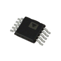
ADP1873ARMZ-0.3-R7 Analog Devices Inc, ADP1873ARMZ-0.3-R7 Datasheet - Page 22

ADP1873ARMZ-0.3-R7
Manufacturer Part Number
ADP1873ARMZ-0.3-R7
Description
300kHz, Light Load Eff Enabled
Manufacturer
Analog Devices Inc
Datasheet
1.ADP1872ARMZ-0.6-R7.pdf
(40 pages)
Specifications of ADP1873ARMZ-0.3-R7
Pwm Type
Current Mode
Number Of Outputs
1
Frequency - Max
300kHz
Duty Cycle
84%
Voltage - Supply
2.75 V ~ 20 V
Buck
Yes
Boost
No
Flyback
No
Inverting
No
Doubler
No
Divider
No
Cuk
No
Isolated
No
Operating Temperature
-40°C ~ 125°C
Package / Case
10-MSOP, Micro10™, 10-uMAX, 10-uSOP
Frequency-max
300kHz
Lead Free Status / RoHS Status
Lead free / RoHS Compliant
Other names
ADP1873ARMZ-0.3-R7TR
Available stocks
Company
Part Number
Manufacturer
Quantity
Price
Company:
Part Number:
ADP1873ARMZ-0.3-R7
Manufacturer:
Analog Devices Inc
Quantity:
1 900
ADP1872/ADP1873
The constant on-time (t
with VIN and V
way as to keep the switching frequency virtually independent
of VIN and V
The t
on-time control loop, making it pseudo-fixed frequency to a first
order. Second-order effects, such as dc losses in the external power
MOSFETs (see the Efficiency Consideration section), cause some
variation in frequency vs. load current and line voltage. These
effects are shown in Figure 22 to Figure 33. The variations in
frequency are much reduced compared with the variations
generated when the feedforward technique is not used.
The feedforward technique establishes the following relationship:
where f
600 kHz, and 1.0 MHz).
The t
with VIN and V
pseudo-fixed frequency, see the Pseudo-Fixed Frequency section
for additional information. To allow headroom for VIN/V
sensing, the following two equations must be adhered to. For
typical applications where V
relevant; however, for lower V
PSEUDO-FIXED FREQUENCY
The ADP1872/ADP1873 employ a constant on-time control
scheme. During steady state operation, the switching frequency
stays relatively constant, or pseudo-fixed. This is due to the one-
shot t
duration, given that external conditions such as input voltage,
output voltage, and load current are also at steady state. During
load transients, the frequency momentarily changes for the
duration of the transient event so that the output comes back
within regulation quicker than if the frequency were fixed or if
it were to remain unchanged. After the transient event is complete,
the frequency returns to a pseudo-fixed value to a first-order.
f
ON
V
V
ON
SW
ON
DD
DD
timer senses VIN and V
SW
timer uses a feedforward technique, applied to the constant
= 1/ K
timer that produces a high-side PWM pulse with a fixed
≥ VIN /8 + 1.5
≥ V
is the controller switching frequency (300 kHz,
OUT
t
ON
OUT
/4
OUT
OUT
.
Figure 76. Constant On-Time Timer
. However, this variation occurs in such a
as previously explained. This provides a
ON
INFORMATION
) is not strictly constant because it varies
DD
SW
OUT
DD
is 5 V, these equations are not
, care may be required.
C
to minimize frequency variation
I
VDD
R
(TRIMMED)
VIN
OUT
Rev. A | Page 22 of 40
To illustrate this feature more clearly, this section describes
one such load transient event—a positive load step—in detail.
During load transient events, the high-side driver output pulse
width stays relatively consistent from cycle to cycle; however,
the off-time (DRVL on-time) dynamically adjusts according to
the instantaneous changes in the external conditions mentioned.
When a positive load step occurs, the error amplifier (out of
phase of the output, V
at its output (COMP). In addition, the current-sense amplifier
senses new inductor current information during this positive
load transient event. The error amplifier’s output voltage
reaction is compared to the new inductor current information
that sets the start of the next switching cycle. Because current
information is produced from valley current sensing, it is sensed
at the down ramp of the inductor current, whereas the voltage
loop information is sensed through the counter action upswing
of the error amplifier’s output (COMP).
The result is a convergence of these two signals (see Figure 77),
which allows an instantaneous increase in switching frequency
during the positive load transient event. In summary, a positive
load step causes V
transient up and therefore shortens the off time. This resulting
increase in frequency during a positive load transient helps to
quickly bring V
window.
Similarly, a negative load step causes the off time to lengthen in
response to V
demagnetizing phase, helping to bring V
In this case, the switching frequency decreases, or experiences a
foldback, to help facilitate output voltage recovery.
Because the ADP1872/ADP1873 has the ability to respond
rapidly to sudden changes in load demand, the recovery period
in which the output voltage settles back to its original steady
state operating point is much quicker than it would be for a
fixed-frequency equivalent . Therefore, using a pseudo-fixed
frequency, results in significantly better load transient
performance than using a fixed frequency.
PWM OUTPUT
ERROR AMP
OUTPUT
CS AMP
OUTPUT
Figure 77. Load Transient Response Operation
OUT
LOAD CURRENT
OUT
DEMAND
rising. This effectively increases the inductor
OUT
back up in value and within the regulation
f
to transient down, which causes COMP to
SW
OUT
) produces new voltage information
>
f
SW
OUT
VALLEY
TRIP POINTS
to within regulation.


