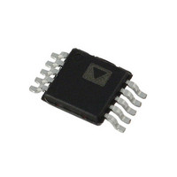
ADP1873ARMZ-0.3-R7 Analog Devices Inc, ADP1873ARMZ-0.3-R7 Datasheet - Page 27

ADP1873ARMZ-0.3-R7
Manufacturer Part Number
ADP1873ARMZ-0.3-R7
Description
300kHz, Light Load Eff Enabled
Manufacturer
Analog Devices Inc
Datasheet
1.ADP1872ARMZ-0.6-R7.pdf
(40 pages)
Specifications of ADP1873ARMZ-0.3-R7
Pwm Type
Current Mode
Number Of Outputs
1
Frequency - Max
300kHz
Duty Cycle
84%
Voltage - Supply
2.75 V ~ 20 V
Buck
Yes
Boost
No
Flyback
No
Inverting
No
Doubler
No
Divider
No
Cuk
No
Isolated
No
Operating Temperature
-40°C ~ 125°C
Package / Case
10-MSOP, Micro10™, 10-uMAX, 10-uSOP
Frequency-max
300kHz
Lead Free Status / RoHS Status
Lead free / RoHS Compliant
Other names
ADP1873ARMZ-0.3-R7TR
Available stocks
Company
Part Number
Manufacturer
Quantity
Price
Company:
Part Number:
ADP1873ARMZ-0.3-R7
Manufacturer:
Analog Devices Inc
Quantity:
1 900
THERMAL CONSIDERATIONS
The ADP1872/ADP1873 are used for dc-to-dc, step down, high
current applications that have an on-board controller and on-board
MOSFET drivers. Because applications may require up to 20 A of
load current delivery and be subjected to high ambient temperature
surroundings, the selection of external upper side and lower side
MOSFETs must be associated with careful thermal consideration
to not exceed the maximum allowable junction temperature
of 125°C. To avoid permanent or irreparable damage if the
junction temperature reaches or exceeds 155°C, the part enters
thermal shutdown, turning off both external MOSFETs, and
does not re-enable until the junction temperature cools to 140°C
(see the Thermal Shutdown section).
The maximum junction temperature allowed for the ADP1872/
ADP1873 ICs is 125°C. This means that the sum of the ambient
temperature (T
is caused by the thermal impedance of the package and the internal
power dissipation, should not exceed 125°C, as dictated by
where:
T
T
dissipated from within.
T
The rise in package temperature is directly proportional to its
thermal impedance characteristics. The following equation
represents this proportionality relationship:
where:
θ
the outside surface of the die, where it meets the surrounding air.
P
The bulk of the power dissipated is due to the gate capacitance
of the external MOSFETs. The power loss equation of the
MOSFET drivers (see the MOSFET Driver Loss section in the
Efficiency Consideration section) is
where:
C
C
I
lower side drivers.
V
minus the rectifier drop (see Figure 80)).
V
BIAS
JA
J
R
A
DR (LOSS)
upperFET
lowerFET
DR
DD
is the maximum junction temperature.
is the rise in package temperature due to the power
is the ambient temperature.
is the thermal resistance of the package from the junction to
is the driver bias voltage (that is, the low input voltage (V
is the dc current (2 mA) flowing into the upper side and
is the bias voltage
T
T
P
(f
DR (LOSS)
J
R
SW
= T
= θ
is the input gate capacitance of the lower side MOSFET.
is the input gate capacitance of the upper side MOSFET.
is the overall power dissipated by the IC.
C
lowerFET
R
JA
× T
× P
= [V
A
V
) and the rise in package temperature (T
A
DR (LOSS)
DD
DR
+ I
× (f
BIAS
SW
C
)]
upperFET
V
DR
+ I
BIAS
)] + [V
DD
×
R
), which
Rev. A | Page 27 of 40
DD
)
For example, if the external MOSFET characteristics are θ
(10-lead MSOP) = 171.2°C/W, f
C
then the power loss is
The rise in package temperature is
Assuming a maximum ambient temperature environment of 85°C,
the junction temperature is
which is below the maximum junction temperature of 125°C.
DESIGN EXAMPLE
The ADP1872/ADP1873 are easy to use, requiring only a few
design criteria. For example, the example outlined in this section
uses only four design criteria: V
VIN = 12 V (typical), and f
Input Capacitor
The maximum input voltage ripple is usually 1% of the
minimum input voltage (11.8 V × 0.01 = 120 mV).
Choose five 22 μF ceramic capacitors. The overall ESR of five
22 μF ceramic capacitors is less than 1 mΩ.
Inductor
Determining inductor ripple current amplitude:
so calculating for the inductor value
upperFET
P
(f
= [5.12 × (300 × 10
[5.5 × (300 × 10
= 77.13 mW
T
= 171.2°C × 77.13 mW
= 13.2°C
T
V
V
= 120 mV − (15 A × 0.001) = 45 mV
= 120 μF
I
P
= 1.03 μH
C
Δ
L
=
RMS
DR (LOSS)
R
J
CIN
SW
RIPP
MAX, RIPPLE
IN,
I ≈
= T
=
= 3.3 nF, C
(
= θ
L
5
13
C
min
= I
= (I
(
lowerFET
= 120 mV
V
V
JA
R
2 .
=
LOAD
I
IN
× T
×
× P
RMS
LOAD
= [V
V
Δ
4
3
,
300
MAX
f
I
= V
V
/2 = 7.5 A
A
)
−
SW
DR (LOSS)
L
2
I
DD
= 13.2°C + 85°C = 98.2°C
DR
LOAD
1
lowerFET
× ESR = (7.5A)
×
V
= 5 A
×
8 .
RIPP
−
+ I
MAX
10
× (f
f
3
SW
V
V
,
×3.3 × 10
MAX
− (I
3
BIAS
OUT
,
)
= 3.3 nF, V
SW
RIPPLE
3
×
× 3.3 × 10
C
)]
LOAD, MAX
)
13
SW
upperFET
1
×
8 .
=
2 .
= 300 kHz.
OUT
V
−9
4
V
SW
V
IN,
V
×
2
V
OUT
× 5.5 + 0.002)]
= 1.8 V, I
DR
ADP1872/ADP1873
× 1 mΩ = 56.25 mW
= 300 kHz, I
300
MAX
× ESR)
DR
−9
= 5.12 V, and V
+ I
× 5.12 + 0.002)] +
×
15
10
BIAS
3
LOAD
A
×
)] + [V
105
= 15 A (pulsing),
BIAS
mV
DD
= 2 mA,
DD
×
= 5.5 V,
JA


