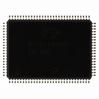
CY7C1480V33-167AXC Cypress Semiconductor Corp, CY7C1480V33-167AXC Datasheet - Page 20

CY7C1480V33-167AXC
Manufacturer Part Number
CY7C1480V33-167AXC
Description
CY7C1480V33-167AXC
Manufacturer
Cypress Semiconductor Corp
Datasheet
1.CY7C1480V33-167AXC.pdf
(31 pages)
Specifications of CY7C1480V33-167AXC
Format - Memory
RAM
Memory Type
SRAM - Synchronous
Memory Size
72M (2M x 36)
Speed
167MHz
Interface
Parallel
Voltage - Supply
3.135 V ~ 3.6 V
Operating Temperature
0°C ~ 70°C
Package / Case
100-LQFP
Density
72Mb
Access Time (max)
3.4ns
Sync/async
Synchronous
Architecture
SDR
Clock Freq (max)
167MHz
Operating Supply Voltage (typ)
3.3V
Address Bus
21b
Package Type
TQFP
Operating Temp Range
0C to 70C
Number Of Ports
4
Supply Current
450mA
Operating Supply Voltage (min)
3.135V
Operating Supply Voltage (max)
3.6V
Operating Temperature Classification
Commercial
Mounting
Surface Mount
Pin Count
100
Word Size
36b
Number Of Words
2M
Lead Free Status / RoHS Status
Lead free / RoHS Compliant
Lead Free Status / RoHS Status
Lead free / RoHS Compliant
Other names
428-2169
CY7C1480V33-167AXC
CY7C1480V33-167AXC
Available stocks
Company
Part Number
Manufacturer
Quantity
Price
Company:
Part Number:
CY7C1480V33-167AXC
Manufacturer:
CYPRESS
Quantity:
101
Company:
Part Number:
CY7C1480V33-167AXC
Manufacturer:
Cypress Semiconductor Corp
Quantity:
10 000
Company:
Part Number:
CY7C1480V33-167AXCT
Manufacturer:
Cypress Semiconductor Corp
Quantity:
10 000
Document Number: 38-05283 Rev. *J
AC Test Loads and Waveforms
Capacitance
Thermal Resistance
Note
C
C
C
C
C
14. Tested initially and after any design or process change that may affect these parameters.
ADDRESS
DATA
CTRL
CLK
I/O
OUTPUT
OUTPUT
Parameter
Parameter
3.3V I/O Test Load
2.5V I/O Test Load
Θ
Θ
JA
JC
[14]
Z
Z
Address Input Capacitance
Data Input Capacitance
Control Input Capacitance
Clock Input Capacitance
Input/Output Capacitance
0
0
Thermal Resistance
(Junction to Ambient)
Thermal Resistance
(Junction to Case)
= 50Ω
= 50Ω
(a)
(a)
Description
V
Description
V
[14]]
L
L
= 1.25V
= 1.5V
R
R
L
L
= 50Ω
= 50Ω
OUTPUT
OUTPUT
3.3V
2.5V
INCLUDING
INCLUDING
Test conditions follow
standard test methods and
procedures for measuring
thermal impedance,
according to EIA/JESD51.
JIG AND
JIG AND
SCOPE
SCOPE
T
A
5 pF
5 pF
Test Conditions
Test Conditions
= 25°C, f = 1 MHz,
V
V
DDQ
DD
= 3.3V
(b)
(b)
= 2.5V
R = 317Ω
R = 1667Ω
R = 351Ω
R = 1538Ω
100 TQFP
Package
100 TQFP
V
24.63
GND
GND
V
DDQ
2.28
Max.
DDQ
6
5
8
6
5
≤ 1 ns
≤ 1 ns
10%
10%
165 FBGA
165 FBGA
Package
16.3
ALL INPUT PULSES
ALL INPUT PULSES
Max.
2.1
6
5
8
6
5
90%
90%
CY7C1480V33
CY7C1482V33
CY7C1486V33
(c)
(c)
209 FBGA
209 FBGA
Package
Max.
15.2
1.7
6
5
8
6
5
Page 20 of 31
90%
90%
10%
10%
°C/W
°C/W
≤ 1 ns
≤ 1 ns
Unit
Unit
pF
pF
pF
pF
pF
[+] Feedback


