J111,126 NXP Semiconductors, J111,126 Datasheet - Page 2
J111,126
Manufacturer Part Number
J111,126
Description
TRANSISTOR N-CH 40V 50MA SOT54
Manufacturer
NXP Semiconductors
Datasheet
1.J112126.pdf
(6 pages)
Specifications of J111,126
Package / Case
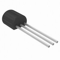
TO-226-3, TO-92-3 (TO-226AA)
Current - Drain (idss) @ Vds (vgs=0)
20mA @ 15V
Drain To Source Voltage (vdss)
40V
Fet Type
N-Channel
Voltage - Breakdown (v(br)gss)
40V
Voltage - Cutoff (vgs Off) @ Id
10V @ 1µA
Input Capacitance (ciss) @ Vds
6pF @ 10V (VGS)
Resistance - Rds(on)
30 Ohm
Mounting Type
Through Hole
Power - Max
400mW
Configuration
Single
Mounting Style
Through Hole
Transistor Polarity
N-Channel
Drain Source Voltage Vds
40 V
Gate-source Cutoff Voltage
3 V
Gate-source Breakdown Voltage
40 V
Drain Current (idss At Vgs=0)
20 mA
Power Dissipation
400 mW
Lead Free Status / RoHS Status
Lead free / RoHS Compliant
Other names
568-5810-2
J111,126
J111,126


Philips Semiconductors
DESCRIPTION
Symmetrical silicon n-channel
junction FETs in plastic TO-92
envelopes. They are intended for
applications such as analog switches,
choppers, commutators etc.
FEATURES
PINNING
Note: Drain and source are
interchangeable.
QUICK REFERENCE DATA
July 1993
1 = gate
2 = source
3 = drain
Drain-source voltage
Drain current
Total power dissipation
Gate-source cut-off voltage
Drain-source on-state resistance
High speed switching
Interchangeability of drain and
source connections
Low R
N-channel silicon field-effect transistors
V
up to T
V
V
DS
DS
DS
= 15 V; V
= 5 V; I
= 0.1 V; V
DS on
amb
at zero gate voltage
= 50 C
D
= 1 A
GS
GS
= 0
= 0
I
P
R
DSS
handbook, halfpage
V
V
tot
DS on
DS
GS off
Fig.1 Simplified outline and symbol, TO-92.
2
1
2
3
max.
min.
max.
min.
max.
max.
J111
400
40
20
30
10
3
MAM042
J112
J111; J112; J113
400
g
40
50
5
5
1
Product specification
J113
400
100
0.5
d
s
40
2
3
V
mA
mW
V
V
Related parts for J111,126
Image
Part Number
Description
Manufacturer
Datasheet
Request
R

Part Number:
Description:
NXP Semiconductors designed the LPC2420/2460 microcontroller around a 16-bit/32-bitARM7TDMI-S CPU core with real-time debug interfaces that include both JTAG andembedded trace
Manufacturer:
NXP Semiconductors
Datasheet:

Part Number:
Description:
NXP Semiconductors designed the LPC2458 microcontroller around a 16-bit/32-bitARM7TDMI-S CPU core with real-time debug interfaces that include both JTAG andembedded trace
Manufacturer:
NXP Semiconductors
Datasheet:
Part Number:
Description:
NXP Semiconductors designed the LPC2468 microcontroller around a 16-bit/32-bitARM7TDMI-S CPU core with real-time debug interfaces that include both JTAG andembedded trace
Manufacturer:
NXP Semiconductors
Datasheet:
Part Number:
Description:
NXP Semiconductors designed the LPC2470 microcontroller, powered by theARM7TDMI-S core, to be a highly integrated microcontroller for a wide range ofapplications that require advanced communications and high quality graphic displays
Manufacturer:
NXP Semiconductors
Datasheet:
Part Number:
Description:
NXP Semiconductors designed the LPC2478 microcontroller, powered by theARM7TDMI-S core, to be a highly integrated microcontroller for a wide range ofapplications that require advanced communications and high quality graphic displays
Manufacturer:
NXP Semiconductors
Datasheet:
Part Number:
Description:
The Philips Semiconductors XA (eXtended Architecture) family of 16-bit single-chip microcontrollers is powerful enough to easily handle the requirements of high performance embedded applications, yet inexpensive enough to compete in the market for hi
Manufacturer:
NXP Semiconductors
Datasheet:
Part Number:
Description:
The XA-S3 device is a member of Philips Semiconductors? XA(eXtended Architecture) family of high performance 16-bitsingle-chip microcontrollers
Manufacturer:
NXP Semiconductors
Datasheet:

Part Number:
Description:
The NXP BlueStreak LH75401/LH75411 family consists of two low-cost 16/32-bit System-on-Chip (SoC) devices
Manufacturer:
NXP Semiconductors
Datasheet:
Part Number:
Description:
The NXP LPC3130/3131 combine an 180 MHz ARM926EJ-S CPU core, high-speed USB2
Manufacturer:
NXP Semiconductors
Datasheet:
Part Number:
Description:
The NXP LPC3141 combine a 270 MHz ARM926EJ-S CPU core, High-speed USB 2
Manufacturer:
NXP Semiconductors
Part Number:
Description:
The NXP LPC3143 combine a 270 MHz ARM926EJ-S CPU core, High-speed USB 2
Manufacturer:
NXP Semiconductors

Part Number:
Description:
The NXP LPC3152 combines an 180 MHz ARM926EJ-S CPU core, High-speed USB 2
Manufacturer:
NXP Semiconductors
Part Number:
Description:
The NXP LPC3154 combines an 180 MHz ARM926EJ-S CPU core, High-speed USB 2
Manufacturer:
NXP Semiconductors

Part Number:
Description:
Standard level N-channel enhancement mode Field-Effect Transistor (FET) in a plastic package using NXP High-Performance Automotive (HPA) TrenchMOS technology
Manufacturer:
NXP Semiconductors
Datasheet: