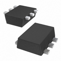
SSM6P35FE(TE85L,F) Toshiba, SSM6P35FE(TE85L,F) Datasheet - Page 2

SSM6P35FE(TE85L,F)
Manufacturer Part Number
SSM6P35FE(TE85L,F)
Description
MOSFET DUAL P-CH 20V .1A ES6
Manufacturer
Toshiba
Datasheet
1.SSM6P35FETE85LF.pdf
(5 pages)
Specifications of SSM6P35FE(TE85L,F)
Fet Type
2 P-Channel (Dual)
Fet Feature
Logic Level Gate
Rds On (max) @ Id, Vgs
8 Ohm @ 50mA, 4V
Drain To Source Voltage (vdss)
20V
Current - Continuous Drain (id) @ 25° C
100mA
Vgs(th) (max) @ Id
1V @ 1mA
Input Capacitance (ciss) @ Vds
12.2pF @ 3V
Power - Max
150mW
Mounting Type
Surface Mount
Package / Case
ES6
Lead Free Status / RoHS Status
Lead free / RoHS Compliant
Gate Charge (qg) @ Vgs
-
Other names
SSM6P35FE(TE85LF)TR
Electrical Characteristics
Switching Time Test Circuit
Usage Considerations
SSM6P35FE). Then, for normal switching operation, V
V
Handling Precaution
When handling individual devices that are not yet mounted on a circuit board, make sure that the environment is
protected against electrostatic discharge. Operators should wear antistatic clothing, and containers and other objects that
come into direct contact with devices should be made of antistatic materials.
th.
Let V
Take this into consideration when using the device.
Gate leakage current
Drain–source breakdown voltage
Drain cutoff current
Gate threshold voltage
Forward transfer admittance
Drain–source ON-resistance
Input capacitance
Reverse transfer capacitance
Output capacitance
Switching time
Drain–source forward voltage
Note 2: Pulse test
(a) Test Circuit
This relationship can be expressed as: V
−
2.5V
th
0
be the voltage applied between gate and source that causes the drain current (I
10 μs
Characteristics
V
D.U. ≤ 1%
V
(Z
Common Source
Ta = 25°C
DD
IN
out
: t
= -3 V
r
= 50 Ω)
, t
f
Turn-on time
Turn-off time
< 5 ns
IN
(Ta = 25°C) (Common to the Q1, Q2)
R
V
OUT
L
DD
(Common to the Q1, Q2)
V
R
Symbol
(BR) DSS
DS (ON)
⏐Y
V
I
I
C
C
C
GSS
DSS
V
t
t
DSF
oss
on
off
rss
iss
GS(off)
th
fs
⏐
< V
V
I
V
V
V
I
I
I
I
V
V
V
I
D
D
D
D
D
D
(b) V
(c) V
GS
DS
DS
DS
DS
DD
GS
GS(on)
= -0.1 mA, V
= -50 mA, V
= -50 mA, V
= -5 mA, V
= -2 mA, V
= 100 mA, V
th
= -20 V, V
= -3 V, I
= -3 V, I
= -3 V, V
= ±10 V, V
= -3 V, I
= 0 to -2.5 V
< V
2
OUT
IN
GS(on).
must be higher than V
Test Condition
D
D
D
GS
GS
GS
GS
GS
GS
= -1 mA
= -50 mA
= -50 mA,
GS
GS
DS
= -1.5 V
= -1.2 V
= 0 V, f = 1 MHz
= -4 V
= -2.5 V
= 0 V
= 0 V
= 0 V
= 0 V
V
V
DD
DS (ON)
−2.5 V
0 V
(Note 2)
(Note 2)
(Note 2)
(Note 2)
(Note 2)
(Note 2)
th,
and V
t
on
10%
D
) to below (−1 mA for the
-0.4
Min
-20
77
⎯
⎯
⎯
⎯
⎯
⎯
⎯
⎯
⎯
⎯
⎯
⎯
t
GS(off)
r
90%
10%
Typ.
12.2
10.4
0.83
175
251
4.3
5.6
8.2
6.5
must be lower than
11
⎯
⎯
⎯
⎯
⎯
SSM6P35FE
t
90%
off
2008-03-14
Max
±10
-1.0
t
1.2
11
22
44
f
⎯
⎯
⎯
⎯
⎯
⎯
⎯
-1
8
Unit
mS
μA
μA
pF
ns
Ω
V
V
V


