TPCP8301(TE85L,F,M Toshiba, TPCP8301(TE85L,F,M Datasheet
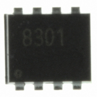
MOSFET P-CH DUAL 20V 5A PS-8

TPCP8301(TE85L,F,M

Manufacturer Part Number
TPCP8301(TE85L,F,M
Description
MOSFET P-CH DUAL 20V 5A PS-8
Manufacturer
Toshiba
Datasheet

Specifications of TPCP8301(TE85L,F,M

Fet Type
2 P-Channel (Dual)
Fet Feature
Logic Level Gate
Rds On (max) @ Id, Vgs
31 mOhm @ 2.5A, 4.5V
Drain To Source Voltage (vdss)
20V
Current - Continuous Drain (id) @ 25° C
5A
Vgs(th) (max) @ Id
1.2V @ 200µA
Gate Charge (qg) @ Vgs
20nC @ 5V
Input Capacitance (ciss) @ Vds
1500pF @ 10V
Power - Max
580mW
Mounting Type
Surface Mount
Package / Case
PS-8
Configuration
Dual Dual Drain
Transistor Polarity
P-Channel
Resistance Drain-source Rds (on)
0.031 Ohms
Drain-source Breakdown Voltage
- 20 V
Gate-source Breakdown Voltage
+/- 12 V
Continuous Drain Current
5 A
Power Dissipation
1.48 W
Maximum Operating Temperature
+ 150 C
Minimum Operating Temperature
- 55 C
Lead Free Status / RoHS Status
Lead free / RoHS Compliant
Other names
TPCP8301TE85LFMTR
Lithium Ion Battery Applications
Notebook PC Applications
Portable Equipment Applications
Absolute Maximum Ratings
Circuit Configuration
Lead (Pb)-free
Small footprint due to small and thin package
Low drain-source ON-resistance: R
High forward transfer admittance: |Y
Low leakage current: I
Enhancement model: V
Drain-source voltage
Drain-gate voltage (R
Gate-source voltage
Drain current
Drain power
dissipation
(t = 5 s) (Note 2a) Single-device value at
Drain power
dissipation
(t = 5 s) (Note 2b) Single-device value at
Single-pulse avalanche energy
Avalanche current
Repetitive avalanche energy
Single-device value at dual operation
Channel temperature
Storage temperature range
Note: For Notes 1 to 6, see the next page.
This transistor is an electrostatic-sensitive device. Handle with care.
Using continuously under heavy loads (e.g. the application of high temperature/current/voltage and the significant change in
temperature, etc.) may cause this product to decrease in the reliability significantly even if the operating conditions (i.e.
operating temperature/current/voltage, etc.) are within the absolute maximum ratings. Please design the appropriate
reliability upon reviewing the Toshiba Semiconductor Reliability Handbook (“Handling Precautions”/Derating Concept and
Methods) and individual reliability data (i.e. reliability test report and estimated failure rate, etc).
Characteristic
TOSHIBA Field Effect Transistor Silicon P Channel MOS Type (U-MOSⅣ)
8
1
DC
Pulse
Single-device operation
dual operation (Note 3b)
Single-device operation
dual operation (Note 3b)
GS
2
7
DSS
= 20 kΩ)
th
= −0.5 to −1.2V (V
(Note 2a, 3b, 5)
= −10 µA (max) (V
6
3
(Note 3a)
(Note 3a)
(Note 1)
(Note 1)
(Note 4)
DS(ON)
fs
(Ta = 25°C)
| = 14 S (typ.)
5
4
TPCP8301
= 25 mΩ (typ.)
Symbol
DS
V
V
P
P
P
P
V
E
E
T
DS
T
I
I
DGR
D (1)
D (2)
D (1)
D (2)
DSS
GSS
DP
AR
= −10 V, I
I
AS
AR
stg
D
ch
= −20 V)
−55 to 150
D
1
Rating
= −200 µA)
1.48
1.23
0.58
0.36
0.12
−20
−20
±12
−20
150
6.5
−5
−5
Marking
Unit
mJ
mJ
°C
°C
W
V
V
V
A
A
8
(Note 6)
1
Weight: 0.017 g (typ.)
JEDEC
JEITA
TOSHIBA
1. Source1
2. Gate1
3. Source2
4. Gate2
8301
0.475
7
S
2
0.33±0.05
8
1
0.025
0.65
6
3
2.9±0.1
0.17±0.02
Lot No.
0.05
5. Drain2
6. Drain2
7. Drain1
8. Drain1
S
M
2-3V1G
TPCP8301
5
4
5
A
2006-11-17
4
B
0.28
1.12
1.12
0.28
A
0.8±0.05
Unit: mm
+0.13
+0.13
+0.1
+0.1
-0.11
0.05
-0.11
-0.12
-0.12
M
B

Related parts for TPCP8301(TE85L,F,M

TPCP8301(TE85L,F,M Summary of contents

Page 1

... Please design the appropriate reliability upon reviewing the Toshiba Semiconductor Reliability Handbook (“Handling Precautions”/Derating Concept and Methods) and individual reliability data (i.e. reliability test report and estimated failure rate, etc). ...

Page 2

Thermal Characteristics Characteristic Single-device operation Thermal resistance, (Note 3a) channel to ambient ( (Note 2a) Single-device value at dual operation (Note 3b) Single-device operation Thermal resistance, (Note 3a) channel to ambient ( (Note 2b) ...

Page 3

Electrical Characteristics Characteristic Gate leakage current Drain cutoff current Drain-source breakdown voltage Gate threshold voltage Drain-source ON-resistance Forward transfer admittance Input capacitance Reverse transfer capacitance Output capacitance Rise time Turn-on time Switching time Fall time Turn-off time ...

Page 4

I – −10 Common source −10 −2.5 − 25°C −8 Pulse test −8 −4 −6 −2.0 −6 −1.8 −4 −1.6 − −1 −0.2 −0.4 −0.6 −0.8 0 Drain−source voltage V ...

Page 5

R – (ON) 100 Common source Pulse test − −2 − −1 −2 −4.5 V ...

Page 6

Safe operating area −100 Single-device value at dual operation (Note 3b max (Pulse) * − −1 * Single pulse Ta = 25°C Curves must be derated ...

Page 7

TPCP8301 2006-11-17 ...

Related keywords