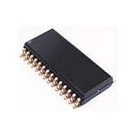
UDA1342TSDB NXP Semiconductors, UDA1342TSDB Datasheet - Page 15

UDA1342TSDB
Manufacturer Part Number
UDA1342TSDB
Description
Audio CODECs AUDIO CODEC MINIDISC
Manufacturer
NXP Semiconductors
Datasheet
1.UDA1342TSN1512.pdf
(45 pages)
Specifications of UDA1342TSDB
Number Of Adc Inputs
4
Number Of Dac Outputs
2
Conversion Rate
110 KSPs
Interface Type
Serial (I2C), L3
Resolution
24 bit
Operating Supply Voltage
2.7 V to 3.6 V
Maximum Operating Temperature
+ 85 C
Mounting Style
SMD/SMT
Package / Case
SSOP-28
Minimum Operating Temperature
- 40 C
Number Of Channels
6
Snr
100 dB
Supply Current
20 mA
Lead Free Status / RoHS Status
Lead free / RoHS Compliant
Other names
UDA1342TS/N1,512
NXP Semiconductors
Information transfer via the microcontroller bus is
organized LSB first and in accordance with the so called
‘L3’ format, in which two different modes of operation can
be distinguished: address mode and data transfer mode.
Important:
• When the device is powered-up, at least one L3CLOCK
• Inside the microcontroller there is a hand-shake
• The L3-bus interface is designed in such a way that data
8.15.2
The device address mode is used to select a device for
subsequent data transfer. The address mode is
characterized by L3MODE being LOW and a burst of
8 pulses on L3CLOCK, accompanied by 8 bits. The
fundamental timing in the address mode is shown in
Fig.13.
The device address consists of one byte, which is split up
in two parts (see Table 10):
• Bits 0 and 1 are called Data Operation Mode (DOM) bits
• Bits 2 to 7 represent a 6-bit device address.
Table 10 L3-bus interface slave address
The UDA1342TS can be set to different addresses
(00 1000 or 10 1000) by setting pin IPSEL to HIGH or
LOW level. In the event that the device receives a different
address, it will deselect its microcontroller interface logic.
Basically, 2 types of data transfer can be defined: data
transfer to the device and data transfer from the device
(see Table 11).
2000 Jul 31
LSB BIT 1 BIT 2 BIT 3 BIT 4 BIT 5 BIT 6 MSB
R/W
pulse must be sent to the L3-bus interface to wake-up
the interface prior to sending information to the device.
This is only needed once after the device is powered-up.
mechanism which handles proper data transfer from the
microcontroller clock to destination clock domains. This
means that when data is sent to the microcontroller
interface, the system clock must be running.
is clocked into the device (write mode) on the positive
clock edge, while the device starts the output data (read
mode) on the negative clock edge. The microcontroller
must read the data from the device on the positive clock
edge to ensure the data is always stable.
and represent the type of data transfer
Audio CODEC
DOM
D
1
EVICE ADDRESSING
IPSEL
0
DEVICE ADDRESS
1
0
0
0
15
Table 11 Selection of data transfer
8.15.3
After sending the device address, including the flags (DOM
bits) whether the information is read or written, the data
transfer mode is entered and one byte is sent with the
destination register address (see Table 12) using 7 bits,
and one bit which signals whether information will be read
or written.
The fundamental timing for the data transfer mode is given
in Fig.14.
Table 12 L3-bus register address
Basically there are 3 cases for register addressing:
1. Register addressing for L3-bus write: the first bit is at
2. Prepare read addressing: the first bit of the byte is at
3. Read action itself: in this case the device returns a
Important:
1. Each time a new destination address needs to be
2. When addressing the device for the first time after
LSB BIT 1 BIT 2 BIT 3 BIT 4 BIT 5 BIT 6 MSB
R/W
BIT 0
logic 0 indicating a write action to the destination
register, and is followed by 7 bits indicating the register
address.
logic 1, signalling data will be read from the register
indicated.
register address prior to sending data from that
register. When the first bit of the byte is at logic 0, the
register address was valid and if the first bit is at logic 1
the register address was invalid.
written, the device address must be sent again.
power-up of the device, at least one L3CLOCK cycle
must be given to enable the L3-bus interface.
0
1
0
1
DOM
A6
R
EGISTER ADDRESSING
BIT 1
0
0
1
1
A5
not used
not used
data write or prepare read
data read
A4
A3
TRANSFER
UDA1342TS
Product specification
A2
A1
A0


