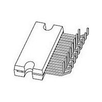
TDA8566Q/N2C NXP Semiconductors, TDA8566Q/N2C Datasheet - Page 8

TDA8566Q/N2C
Manufacturer Part Number
TDA8566Q/N2C
Description
Audio Amplifiers 2X25W BTL STEREO RADIO PWR AMP
Manufacturer
NXP Semiconductors
Datasheet
1.TDA8566QN2C.pdf
(21 pages)
Specifications of TDA8566Q/N2C
Product
Class-B
Output Power
55 W
Available Set Gain
26 dB
Common Mode Rejection Ratio (min)
60 dB
Thd Plus Noise
0.05 %
Operating Supply Voltage
14.4 V
Maximum Power Dissipation
60000 mW
Maximum Operating Temperature
+ 85 C
Mounting Style
Through Hole
Audio Load Resistance
4 Ohms
Input Signal Type
Differential
Minimum Operating Temperature
- 40 C
Output Signal Type
Differential
Supply Type
Single
Supply Voltage (max)
18 V
Supply Voltage (min)
6 V
Output Type
2-Channel Stereo
Package / Case
DBS17P
Operational Class
Class-B
Audio Amplifier Output Configuration
2-Channel Stereo
Output Power (typ)
55x2@2OhmW
Audio Amplifier Function
Speaker
Total Harmonic Distortion
0.05@4Ohm@1W%
Single Supply Voltage (typ)
14.4V
Dual Supply Voltage (typ)
Not RequiredV
Power Supply Requirement
Single
Power Dissipation
60W
Rail/rail I/o Type
No
Single Supply Voltage (min)
6V
Single Supply Voltage (max)
18V
Dual Supply Voltage (min)
Not RequiredV
Dual Supply Voltage (max)
Not RequiredV
Operating Temp Range
-40C to 85C
Operating Temperature Classification
Industrial
Mounting
Through Hole
Pin Count
17
Package Type
DBS17P
Lead Free Status / RoHS Status
Lead free / RoHS Compliant
Other names
TDA8566Q/N2C,112
NXP Semiconductors
8. Limiting values
9. Thermal characteristics
TDA8566_6
Product data sheet
7.6 Differential inputs
The input stage is a high-impedance fully differential balanced input stage that is also
capable of operating in a single-ended mode with one of the inputs capacitively coupled to
an audio ground. It should be noted that if a source resistance is added (input voltage
dividers) the CMRR degrades to lower values.
Table 5.
In accordance with the Absolute Maximum Rating System (IEC 60134).
Table 6.
Thermal characteristics in accordance with IEC 60747-1.
Symbol
V
I
I
T
T
T
V
V
P
Symbol
R
R
OSM
ORM
Fig 7. Equivalent thermal resistance network
stg
vj
amb
P
psc
rp
tot
th(j-c)
th(j-a)
Parameter
supply voltage
non-repetitive peak output
current
repetitive peak output
current
storage temperature
virtual junction temperature
ambient temperature
short-circuit safe voltage
reverse polarity voltage
total power dissipation
Parameter
thermal resistance from junction to case
thermal resistance from junction to ambient in free air
Limiting values
Thermal characteristics
Rev. 06 — 15 October 2007
virtual junction
2
2.2 K/W
Conditions
operating
non-operating
load dump protection;
during 50 ms; t
40 W/2
output 1
case
0.2 K/W
stereo BTL car radio power amplifier
output 2
r
Conditions
see
001aaa155
2.5 ms
2.2 K/W
Figure 7
Min
-
-
-
-
-
-
-
-
-
55
40
TDA8566
© NXP B.V. 2007. All rights reserved.
Typ
1.3
40
Max
18
30
45
10
7.5
+150
150
+85
18
6.0
60
Unit
K/W
K/W
Unit
V
V
V
A
A
V
V
W
C
C
C
8 of 21


