TDA8566Q NXP Semiconductors, TDA8566Q Datasheet
TDA8566Q
Specifications of TDA8566Q
Available stocks


Related parts for TDA8566Q


TDA8566Q Summary of contents
Page 1
... TDA8566TH1 is a 24-lead small outline plastic package which is pin compatible with the 2 I C-bus controlled amplifier TDA1566TH for one board layout. TDA8566Q is a 17-pin DIL-bent-SIL package. The device contains 2 amplifiers in a Bridge-Tied Load (BTL) configuration. The output power is 2 and 2 diagnostic outputs ...
Page 2
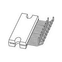
... Name Description TDA8566TH HSOP20 plastic, heatsink small outline package; 20 leads; low stand-off height TDA8566TH1 HSOP24 plastic, heatsink small outline package; 24 leads; low stand-off height TDA8566Q DBS17P plastic DIL-bent-SIL power package; 17 leads (lead length 12 mm) TDA8566_6 Product data sheet 2 Quick reference data = kHz ...
Page 3
... NXP Semiconductors 5. Block diagram IN1+ IN1 n.c. V ref SGND IN2+ IN2 (1) HEATTAB PGND2 (1) Pin HEATTAB is available in TDA8566TH1 only. Fig 1. Block diagram TDA8566_6 Product data sheet 2 mute switch V A 2.3 k mute switch 2 standby switch standby V reference A voltage 1 mute reference 60 60 voltage k k mute ...
Page 4
... Pinning information 6.1 Pinning 20 MODE OUT2 18 17 PGND2 OUT2+ 16 TDA8566TH OUT1 15 PGND1 14 13 OUT1 CLIP 11 Fig 2. Pin configuration TDA8566TH Fig 4. Pin configuration TDA8566Q TDA8566_6 Product data sheet 2 40 W/2 HEATTAB 1 DIAG 2 IN2+ 3 IN2 4 n.c. 5 n.c. 6 n.c. 7 n.c. 8 IN1+ 9 IN1 10 SGND 001aag902 Fig 3. Pin confi ...
Page 5
... Pin description TDA8566Q Pin Description 1 channel 1 input positive 2 channel 1 input negative 3 signal ground 4 clip detection output 5 supply voltage 1 6 channel 1 output positive 7 power ground 1 8 channel 1 output negative 9 not connected Rev. 06 — 15 October 2007 TDA8566 stereo BTL car radio power amplifier ...
Page 6
... The clip detection circuit is disabled in a short-circuit condition fault condition occurs at the outputs, pin CLIP will remain at a HIGH level. The clip detection waveforms are illustrated in TDA8566_6 Product data sheet 2 40 W/2 Pin description TDA8566Q …continued Pin Description 10 channel 2 output positive 11 ...
Page 7
... NXP Semiconductors Fig 5. Clip detection waveforms 7.3 Short-circuit diagnostic (pin DIAG) When a short-circuit occurs at one or more outputs to ground or to the supply voltage, the output stages are switched off until the short-circuit is removed and the device is switched on again (with a delay of approximately 20 ms after the removal of the short-circuit). ...
Page 8
... NXP Semiconductors 7.6 Differential inputs The input stage is a high-impedance fully differential balanced input stage that is also capable of operating in a single-ended mode with one of the inputs capacitively coupled to an audio ground. It should be noted that if a source resistance is added (input voltage dividers) the CMRR degrades to lower values. ...
Page 9
... NXP Semiconductors 10. Static characteristics Table 14 Symbol Supply Operating condition V MODE I MODE Mute condition V MODE Standby condition V MODE I stb Diagnostic V DIAG [1] The circuit is DC adjusted TDA8566_6 Product data sheet 2 Static characteristics = 25 C; measured in test circuit of amb Parameter Conditions supply voltage quiescent current ...
Page 10
... NXP Semiconductors 11. Dynamic characteristics Table 14 otherwise specified. Symbol P o THD B f ro(l) f ro( SVRR n( TDA8566_6 Product data sheet 2 40 W/2 Dynamic characteristics = kHz; measured in test circuit of amb L i Parameter Conditions output power THD = 0.5 % THD = 10 % THD = 13.5 V; THD = 0 13.5 V; THD = THD = 0.5 % ...
Page 11
... NXP Semiconductors Table 14 otherwise specified. Symbol V o(mute) CMRR [1] Dynamic distortion detector active; pin CLIP is LOW. [2] Frequency response externally fixed. [3] V ripple [4] Noise measured in a bandwidth kHz. [5] Common mode rejection ratio measured at the output (over R V common [6] Common mode rejection ratio measured at the output (over R ...
Page 12
... NXP Semiconductors 13. Test information V MODE 220 in1 220 220 in2 220 Fig 9. Stereo BTL test diagram TDA8566_6 Product data sheet MODE P1 IN1 TDA8566 60 k IN1 CLIP V DETECTOR ref SGND DIAGNOSTIC INTERFACE IN2 IN2 PGND1 Rev. 06 — 15 October 2007 TDA8566 40 W/2 stereo BTL car radio power amplifier ...
Page 13
... NXP Semiconductors 14. Package outline HSOP20: plastic, heatsink small outline package; 20 leads; low stand-off height pin 1 index DIMENSIONS (mm are the original dimensions) A (1) UNIT max. 0.08 0.53 3.5 mm 3.5 0.35 0.04 0.40 3.2 Notes 1. Limits per individual lead. 2. Plastic or metal protrusions of 0.25 mm maximum per side are not included. ...
Page 14
... NXP Semiconductors HSOP24: plastic, heatsink small outline package; 24 leads; low stand-off height pin 1 index DIMENSIONS (mm are the original dimensions) A (1) UNIT max. 0.08 0.53 3.5 mm 3.5 0.35 0.04 0.40 3.2 Notes 1. Limits per individual lead. 2. Plastic or metal protrusions of 0.25 mm maximum per side are not included. ...
Page 15
... NXP Semiconductors DBS17P: plastic DIL-bent-SIL power package; 17 leads (lead length 12 mm DIMENSIONS (mm are the original dimensions) UNIT 17.0 4.6 0.75 0.48 24.0 mm 15.5 4.4 0.60 0.38 23.6 Note 1. Plastic or metal protrusions of 0.25 mm maximum per side are not included. OUTLINE VERSION IEC SOT243-1 Fig 12 ...
Page 16
... NXP Semiconductors 15. Soldering This text provides a very brief insight into a complex technology. A more in-depth account of soldering ICs can be found in Application Note AN10365 “Surface mount reflow soldering description” . 15.1 Introduction to soldering Soldering is one of the most common methods through which packages are attached to Printed Circuit Boards (PCBs), to form electrical circuits ...
Page 17
... NXP Semiconductors 15.4 Reflow soldering Key characteristics in reflow soldering are: • Lead-free versus SnPb soldering; note that a lead-free reflow process usually leads to higher minimum peak temperatures (see reducing the process window • Solder paste printing issues including smearing, release, and adjusting the process window for a mix of large and small components on one board • ...
Page 18
... NXP Semiconductors Fig 13. Temperature profiles for large and small components For further information on temperature profiles, refer to Application Note AN10365 “Surface mount reflow soldering description” . TDA8566_6 Product data sheet 2 maximum peak temperature = MSL limit, damage level temperature minimum peak temperature ...
Page 19
... Legal texts have been adapted to the new company name where appropriate. • Section 9 “Thermal characteristics”: changed value of R • Figure 7: values updated • Included TDA8566TH1 and TDA8566Q in the data sheet 20010221 Product specification 20030708 Product specification Rev. 06 — 15 October 2007 40 W/2 stereo BTL car radio power amplifier ...
Page 20
... For detailed and full information see the relevant full data sheet, which is available on request via the local NXP Semiconductors sales office. In case of any inconsistency or conflict with the short data sheet, the full data sheet shall prevail ...
Page 21
... NXP Semiconductors 19. Contents 1 General description . . . . . . . . . . . . . . . . . . . . . . 1 2 Features . . . . . . . . . . . . . . . . . . . . . . . . . . . . . . . 1 3 Quick reference data . . . . . . . . . . . . . . . . . . . . . 2 4 Ordering information . . . . . . . . . . . . . . . . . . . . . 2 5 Block diagram . . . . . . . . . . . . . . . . . . . . . . . . . . 3 6 Pinning information . . . . . . . . . . . . . . . . . . . . . . 4 6.1 Pinning . . . . . . . . . . . . . . . . . . . . . . . . . . . . . . . 4 6.2 Pin description . . . . . . . . . . . . . . . . . . . . . . . . . 5 7 Functional description . . . . . . . . . . . . . . . . . . . 6 7.1 Mode select switch (pin MODE 7.2 Clip detection (pin CLIP 7.3 Short-circuit diagnostic (pin DIAG ...