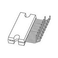
TDA8566Q NXP Semiconductors, TDA8566Q Datasheet - Page 11

TDA8566Q
Manufacturer Part Number
TDA8566Q
Description
Manufacturer
NXP Semiconductors
Datasheet
1.TDA8566Q.pdf
(21 pages)
Specifications of TDA8566Q
Operational Class
Class-B
Audio Amplifier Output Configuration
2-Channel Stereo
Output Power (typ)
55x2@2OhmW
Audio Amplifier Function
Speaker
Total Harmonic Distortion
0.05@4Ohm@1W%
Single Supply Voltage (typ)
14.4V
Dual Supply Voltage (typ)
Not RequiredV
Power Supply Requirement
Single
Power Dissipation
60W
Rail/rail I/o Type
No
Single Supply Voltage (min)
6V
Single Supply Voltage (max)
18V
Dual Supply Voltage (min)
Not RequiredV
Dual Supply Voltage (max)
Not RequiredV
Operating Temp Range
-40C to 85C
Operating Temperature Classification
Industrial
Mounting
Through Hole
Pin Count
17
Package Type
DBS17P
Lead Free Status / Rohs Status
Compliant
Available stocks
Company
Part Number
Manufacturer
Quantity
Price
Company:
Part Number:
TDA8566Q
Manufacturer:
MAXIM
Quantity:
300
Part Number:
TDA8566Q
Manufacturer:
PHILIPS/飞利浦
Quantity:
20 000
Part Number:
TDA8566Q 70039AB
Manufacturer:
NXP/恩智浦
Quantity:
20 000
Company:
Part Number:
TDA8566Q/N2/S438
Manufacturer:
AELTA
Quantity:
27
Company:
Part Number:
TDA8566Q/N2S,112
Manufacturer:
IDT
Quantity:
6 792
NXP Semiconductors
12. Application information
TDA8566_6
Product data sheet
12.1 Diagnostic output
12.2 Mode select switch
Table 8.
V
otherwise specified.
[1]
[2]
[3]
[4]
[5]
[6]
Special care must be taken in the PCB layout to separate pin CLIP from
pins IN1+, IN1 , IN2+ and IN2 to minimize the crosstalk between the CLIP output and
the inputs.
To avoid switch-on plops, it is advisable to keep the amplifier in the mute mode during
in
and results in fast muting when switching off.
Symbol
V
CMRR
P
Fig 8. Mode select switch circuit
o(mute)
150 ms (charging of the input capacitors at pins IN1+, IN1 , IN2+ and IN2 ). The circuit
Figure 8
= 14.4 V; T
Dynamic distortion detector active; pin CLIP is LOW.
Frequency response externally fixed.
V
Noise measured in a bandwidth of 20 Hz to 20 kHz.
Common mode rejection ratio measured at the output (over R
V
Common mode rejection ratio measured at the output (over R
V
ripple
common
common
= V
Parameter
output signal
voltage in mute
common mode
rejection ratio
Dynamic characteristics
slowly ramps-up the voltage at the mode select switch pin when switching on
ripple(max)
3.5 V (RMS); f
3.5 V (RMS); f
amb
= 25 C; R
= 2 V (p-p); R
Rev. 06 — 15 October 2007
i
i
= 100 Hz to 10 kHz; R
= 1 kHz; R
L
= 2 ; f
Conditions
V
R
R
+ V
s
in
s
s
= 0 .
P
S
= 0
= 45 k
= V
s
i
= 45 k . The mismatch of the input coupling capacitors is excluded.
…continued
= 1 kHz; measured in test circuit of
in(max)
2
+
40 W/2
10 k
= 1 V (RMS)
47 F
s
= 0 .
100
100 k
stereo BTL car radio power amplifier
L
L
) with both inputs tied together;
) with both inputs tied together;
mgd102
switch
select
mode
[5]
[6]
Min
-
60
40
Figure
Typ
-
75
-
TDA8566
© NXP B.V. 2007. All rights reserved.
9; unless
Max
2
-
-
11 of 21
Unit
mV
dB
dB


