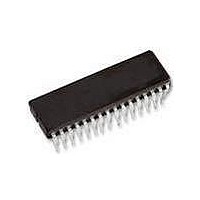
TDA8933T NXP Semiconductors, TDA8933T Datasheet - Page 12

TDA8933T
Manufacturer Part Number
TDA8933T
Description
Audio Amplifiers 2X10W BTL CLASS D AMP+VOLCTRL
Manufacturer
NXP Semiconductors
Datasheet
1.TDA8933TN1112.pdf
(47 pages)
Specifications of TDA8933T
Product
Class-D
Output Power
32 W
Available Set Gain
36 dB
Common Mode Rejection Ratio (min)
75 dB
Thd Plus Noise
0.011 %
Operating Supply Voltage
25 V
Supply Current
0.6 mA
Maximum Power Dissipation
5000 mW
Maximum Operating Temperature
+ 85 C
Mounting Style
SMD/SMT
Audio Load Resistance
16 Ohms
Dual Supply Voltage
+/- 12.5 V
Input Signal Type
Differential
Minimum Operating Temperature
- 40 C
Output Signal Type
Differential, Single
Supply Type
Single or Dual
Supply Voltage (max)
36 V
Supply Voltage (min)
10 V
Output Type
1-Channel Mono or 2-Channel Stereo
Package / Case
SOIC-32
Lead Free Status / RoHS Status
Lead free / RoHS Compliant
Other names
TDA8933T/N1,112
Available stocks
Company
Part Number
Manufacturer
Quantity
Price
Part Number:
TDA8933T
Manufacturer:
NXP/恩智浦
Quantity:
20 000
Company:
Part Number:
TDA8933T/N1
Manufacturer:
AMC
Quantity:
475
Part Number:
TDA8933T/N1
Manufacturer:
NXP/恩智浦
Quantity:
20 000
Part Number:
TDA8933T/N1,118
Manufacturer:
NXP/恩智浦
Quantity:
20 000
NXP Semiconductors
TDA8933_1
Preliminary data sheet
8.5 Diagnostic input and output
8.6 Differential inputs
Whenever one of the protections is triggered, except for TF, pin DIAG is activated to LOW
level (see
approximately 2.4 V. This internal reference supply can deliver approximately 50 A. The
DIAG pin refers to pin CGND.The diagnostic output signal during different short circuit
conditions is illustrated in
device into Fault mode.
For a high common-mode rejection ratio and for maximum flexibility in the application, the
audio inputs are fully differential. By connecting the inputs anti-parallel, the phase of one
of the two channels can be inverted, so that the amplifier can operate as a mono BTL
amplifier. The input configuration for a mono BTL application is illustrated in
In the single-ended configuration it is also recommended to connect the two differential
inputs in anti-phase. This has advantages for the current handling of the power supply at
low signal frequencies and minimizes supply pumping (see also
Fig 5. Diagnostic output for different kinds of short circuit conditions
Fig 6. Input configuration for a mono BTL application
Table
6). An internal reference supply will pull up the open-drain DIAG output to
2.4 V
audio
0 V
input
V
o
Rev. 01 — 15 May 2007
Figure
50 ms
shorted load
IN1P
IN1N
IN2P
IN2N
5. Using pin DIAG as input, a voltage < 0.8 V will put the
50 ms
amplifier
restart
2.4 V
0 V
V
o
OUT1
OUT2
no restart
supply line
Class-D audio amplifier
Section
short to
001aad760
001aad759
TDA8933
© NXP B.V. 2007. All rights reserved.
14.8).
Figure
12 of 47
6.


