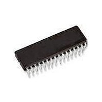
TDA8933T NXP Semiconductors, TDA8933T Datasheet - Page 18

TDA8933T
Manufacturer Part Number
TDA8933T
Description
Audio Amplifiers 2X10W BTL CLASS D AMP+VOLCTRL
Manufacturer
NXP Semiconductors
Datasheet
1.TDA8933TN1112.pdf
(47 pages)
Specifications of TDA8933T
Product
Class-D
Output Power
32 W
Available Set Gain
36 dB
Common Mode Rejection Ratio (min)
75 dB
Thd Plus Noise
0.011 %
Operating Supply Voltage
25 V
Supply Current
0.6 mA
Maximum Power Dissipation
5000 mW
Maximum Operating Temperature
+ 85 C
Mounting Style
SMD/SMT
Audio Load Resistance
16 Ohms
Dual Supply Voltage
+/- 12.5 V
Input Signal Type
Differential
Minimum Operating Temperature
- 40 C
Output Signal Type
Differential, Single
Supply Type
Single or Dual
Supply Voltage (max)
36 V
Supply Voltage (min)
10 V
Output Type
1-Channel Mono or 2-Channel Stereo
Package / Case
SOIC-32
Lead Free Status / RoHS Status
Lead free / RoHS Compliant
Other names
TDA8933T/N1,112
Available stocks
Company
Part Number
Manufacturer
Quantity
Price
Part Number:
TDA8933T
Manufacturer:
NXP/恩智浦
Quantity:
20 000
Company:
Part Number:
TDA8933T/N1
Manufacturer:
AMC
Quantity:
475
Part Number:
TDA8933T/N1
Manufacturer:
NXP/恩智浦
Quantity:
20 000
Part Number:
TDA8933T/N1,118
Manufacturer:
NXP/恩智浦
Quantity:
20 000
NXP Semiconductors
10. Limiting values
11. Thermal characteristics
Table 9.
[1]
[2]
[3]
TDA8933_1
Preliminary data sheet
Symbol
R
th(j-a)
j-lead
j-top
Measured in a JEDEC high K-factor test board (standard EIA/JESD 51-7) in free air with natural convection.
2 layer application board (55 mm
Strongly dependent on where the measurement is taken on the package.
Thermal characteristics
Parameter
thermal resistance from
junction to ambient
thermal characterization
parameter from junction to
lead
thermal characterization
parameter from junction to
top of package
Table 8.
In accordance with the Absolute Maximum Rating System (IEC 60134).
[1]
[2]
[3]
[4]
[5]
Symbol
V
V
I
T
T
T
P
ORM
j
stg
amb
P
x
Measured with respect to pin INREF; V
Measured with respect to pin V
Measured with respect to pin CGND; V
V
Current limiting concept.
SS
= V
45 mm), 35 m copper, FR4 base material in free air with natural convection.
SSP1
Parameter
supply voltage
voltage on pin x
IN1P, IN1N, IN2P, IN2N
OSCREF, OSCIO, TEST
POWERUP, ENGAGE,
DIAG
all other pins
repetitive peak output
current
junction temperature
storage temperature
ambient temperature
power dissipation
Limiting values
= V
Conditions
free air natural convection
SSP2
JEDEC test board
2 layer application board
; V
DD
Rev. 01 — 15 May 2007
= V
DDP1
SSD(HW)
= V
Conditions
asymmetrical supply
maximum output
current limiting
; V
DDP2
x
x
< V
< V
x
< V
.
DD
DD
DD
+ 0.3 V.
+ 0.3 V.
+ 0.3 V.
[1]
[2]
[3]
Min
-
-
-
-
[1]
[2]
[3]
[4]
[5]
Typ
-
41
44
-
-
Min
V
V
V
2.3
-
-
0.3
5
55
40
SSD(HW)
CGND
SS
- 0.3
Class-D audio amplifier
- 0.3
- 0.3 5
Max
44
-
30
8
TDA8933
© NXP B.V. 2007. All rights reserved.
Max
+40
+5
6
V
-
150
+150
+85
5
DD
+ 0.3 V
Unit
K/W
K/W
K/W
K/W
18 of 47
Unit
V
V
V
V
A
W
C
C
C


