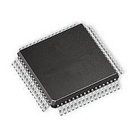
ispPAC-CLK5316S-01TN64I Lattice, ispPAC-CLK5316S-01TN64I Datasheet - Page 34

ispPAC-CLK5316S-01TN64I
Manufacturer Part Number
ispPAC-CLK5316S-01TN64I
Description
Clock Drivers & Distribution ISP 0 Delay Unv Fan- Out Buf-Sngl End I
Manufacturer
Lattice
Datasheet
1.ISPPAC-CLK5308S-01TN48C.pdf
(56 pages)
Specifications of ispPAC-CLK5316S-01TN64I
Minimum Operating Temperature
- 40 C
Mounting Style
SMD/SMT
Maximum Operating Temperature
85 C
Package / Case
TQFP-64
Lead Free Status / RoHS Status
Lead free / RoHS Compliant
Available stocks
Company
Part Number
Manufacturer
Quantity
Price
Company:
Part Number:
ISPPAC-CLK5316S-01TN64I
Manufacturer:
Lattice Semiconductor Corporation
Quantity:
10 000
Lattice Semiconductor
Figure 29. External Feedback Mode and Timing Relationships
Other Features
RESET and Power-up Functions
To ensure proper PLL startup and synchronization of outputs, the ispClock5300S provides both internally gener-
ated and user-controllable external reset signals. An internal reset is generated whenever the device is powered
up. An external reset may be applied by asserting a logic LOW at the RESET pin. Asserting RESET resets all inter-
nal dividers, and will cause the PLL to lose lock. On losing lock, the VCO frequency will begin dropping. The length
of time required to regain lock is related to the length of time for which RESET was asserted.
When the ispClock5300S begins operating from initial power-on, the VCO starts running at a very low frequency
(<100 MHz) which gradually increases as it approaches a locked condition. To prevent invalid outputs from being
applied to the rest of the system, assert OEX or OEY high. This will result in the BANK outputs being held in a high-
impedance state until the OEX or OEY pin is pulled LOW.
After in-system programming the device through the JTAG interface, the reset pin must be activated at least for a
period of t
If the RESET pin is not driven by an external logic it should be pulled up to V
Software-Based Design Environment
Designers can configure the ispClock5300S using Lattice’s PAC-Designer software, an easy to use, Microsoft Win-
dows compatible program. Circuit designs are entered graphically and then verified, all within the PAC-Designer envi-
ronment. Full device programming is supported using PC parallel port I/O operations and a download cable
connected to the serial programming interface pins of the ispClock5300S. A library of configurations is included with
basic solutions and examples of advanced circuit techniques are available. In addition, comprehensive on-line and
printed documentation is provided that covers all aspects of PAC-Designer operation. PAC-Designer is available for
download from the Lattice web site at www.latticesemi.com. The PAC-Designer schematic window, shown in
Figure 30 provides access to all configurable ispClock5300S elements via its graphical user interface. All analog input
and output pins are represented. Static or non-configurable pins such as power, ground and the serial digital interface
are omitted for clarity. Any element in the schematic window can be accessed via mouse operations as well as menu
commands. When completed, configurations can be saved and downloaded to devices.
PLL_RSTW
to reset the device.
Input Reference Clock
OUTPUT
BANK
REF
FBK
FBK
REF
34
t
t
FBK
φ
ispClock5300S
Delay = t
FBK
OUTPUT
ispClock5300S Family Data Sheet
BANK
CCD
through a 10kΩ resistor.


