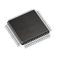
ispPAC-CLK5316S-01TN64I Lattice, ispPAC-CLK5316S-01TN64I Datasheet - Page 46

ispPAC-CLK5316S-01TN64I
Manufacturer Part Number
ispPAC-CLK5316S-01TN64I
Description
Clock Drivers & Distribution ISP 0 Delay Unv Fan- Out Buf-Sngl End I
Manufacturer
Lattice
Datasheet
1.ISPPAC-CLK5308S-01TN48C.pdf
(56 pages)
Specifications of ispPAC-CLK5316S-01TN64I
Minimum Operating Temperature
- 40 C
Mounting Style
SMD/SMT
Maximum Operating Temperature
85 C
Package / Case
TQFP-64
Lead Free Status / RoHS Status
Lead free / RoHS Compliant
Available stocks
Company
Part Number
Manufacturer
Quantity
Price
Company:
Part Number:
ISPPAC-CLK5316S-01TN64I
Manufacturer:
Lattice Semiconductor Corporation
Quantity:
10 000
Lattice Semiconductor
ispClock5300S Family Data Sheet
Detailed Pin Descriptions
VCCO_[0..9], GNDO_[0..9] – These pins provide power and ground for each of the output banks. In the case when
an output bank is unused, its corresponding VCCO pin may be left unconnected or preferably should be tied to
ground. ALL GNDO pins should be tied to ground regardless of whether the associated bank is used or not. When
a bank is used, it should be individually bypassed with a capacitor in the range of 0.01 to 0.1µF as close to its
VCCO and GNDO pins as is practical.
BANK_[0..9]A, BANK_[0..9]B – These pins provide clock output signals. The choice of output driver type (CMOS,
SSTL, etc.) may be selected on a bank-by-bank basis. The output impedance and slew rate may be selected on an
output-by-output basis.
VCCA, GNDA – These pins provide analog supply and ground for the ispClock5300S family’s internal analog cir-
cuitry, and should be bypassed with a 0.1uF capacitor as close to the pins as is practical. To improve noise immu-
nity, it is suggested that the supply to the VCCA pin be isolated from other circuitry with a ferrite bead.
VCCD, GNDD – These pins provide digital supply and ground for the ispClock5300S family’s internal digital cir-
cuitry, and should be bypassed with a 0.1uF capacitor as close to the pins as is practical. To improve noise immu-
nity it is suggested that the supply to the VCCD pins be isolated with ferrite beads.
VCCJ – This pin provides power and a reference voltage for use by the JTAG interface circuitry. It may be set to
allow the ispClock5300S family devices to function in JTAG chains operating at voltages differing from VCCD.
REFA_REFP, REFB_REFN – These input pins provide the inputs for clock signals, and can accommodate either
single ended or differential signal protocols.
REFSEL – This input pin is used to select which clock input pair (REFA or REB) is selected for use as the reference
input. When REFSEL=0, REFA is used, and when REFSEL=1, REFB is used.
VTT_REFA, VTT_REFB – These pins are used to provide a termination voltage for the reference inputs when they
are configured for SSTL or HSTL logic, and should be connected to a suitable voltage supply in those cases.
FBK – This input pin provides feedback sense of the output clock signal, and can accommodate any of the single-
ended logic types.
VTT_FBK – This pin is used to provide a termination voltage for the feedback input when it is configured for SSTL
or HSTL logic, and should be connected to a suitable voltage supply in those cases.
TDO, TDI, TCK, TMS – These pins comprise the ispClock5300S device’s JTAG interface. The signal levels for these
pins are determined by the selection of the VCCJ voltage.
LOCK – This output pin indicates that the device’s PLL is in a locked condition when it goes HIGH.
OEX, OEY – These pins are used to enable the outputs or put them into a high-impedance condition. Each output
may be set so that it is always on, always off, enabled by OEX or enabled by OEY.
PLL_BYPASS – When this pin is pulled LOW, the V-dividers are driven from the output of the device’s VCO, and
the device behaves as a phase-locked loop. When this pin is pulled HIGH, the V-dividers are driven directly from a
selected reference input, and the PLL functions are effectively bypassed.
RESET – When this pin is pulled LOW, all on-board counters are reset, and lock is lost. If the RESET pin is not
driven by an external logic it should be pulled up to V
through a 10kΩ resistor.
CCD
NC – These pins have no internal connection. It is recommended that they be left unconnected.
46


