LAN83C185-JD SMSC, LAN83C185-JD Datasheet
LAN83C185-JD
Specifications of LAN83C185-JD


Related parts for LAN83C185-JD


LAN83C185-JD Summary of contents
Page 1
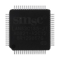
... Integrated DSP with Adaptive Equalizer Baseline Wander (BLW) Correction Media Independent Interface (MII) 802.3u compliant register functions Vendor Specific register functions LAN83C185-JD FOR 64-PIN TQFP PACKAGE LAN83C185-JT FOR 64-PIN TQFP LEAD-FREE ROHS COMPLIANT PACKAGE SMSC LAN83C185 LAN83C185 High Performance Single Chip Low Power 10/100 ...
Page 2
... TORT; NEGLIGENCE OF SMSC OR OTHERS; STRICT LIABILITY; BREACH OF WARRANTY; OR OTHERWISE; WHETHER OR NOT ANY REMEDY OF BUYER IS HELD TO HAVE FAILED OF ITS ESSENTIAL PURPOSE, AND WHETHER OR NOT SMSC HAS BEEN ADVISED OF THE POSSIBILITY OF SUCH DAMAGES. Revision 0.8 (06-12-08) High Performance Single Chip Low Power 10/100 Ethernet Physical Layer Transceiver (PHY) 2 DATASHEET Datasheet SMSC LAN83C185 ...
Page 3
... Re-starting Auto-negotiation . . . . . . . . . . . . . . . . . . . . . . . . . . . . . . . . . . . . . . . . . . . . . . 25 4.7.3 Disabling Auto-negotiation 4.7.4 Half vs. Full Duplex . . . . . . . . . . . . . . . . . . . . . . . . . . . . . . . . . . . . . . . . . . . . . . . . . . . . . 25 4.8 PHY Management Control . . . . . . . . . . . . . . . . . . . . . . . . . . . . . . . . . . . . . . . . . . . . . . . . . . . . . . . 25 4.8.1 Serial Management Interface (SMI Chapter 5 Registers . . . . . . . . . . . . . . . . . . . . . . . . . . . . . . . . . . . . . . . . . . . . . . . . . . . . . . . . . 27 5.1 SMI Register Mapping . . . . . . . . . . . . . . . . . . . . . . . . . . . . . . . . . . . . . . . . . . . . . . . . . . . . . . . . . . 33 5.2 SMI Register Format 5.3 Management Interrupt . . . . . . . . . . . . . . . . . . . . . . . . . . . . . . . . . . . . . . . . . . . . . . . . . . . . . . . . . . 42 5.4 Miscellaneous Functions . . . . . . . . . . . . . . . . . . . . . . . . . . . . . . . . . . . . . . . . . . . . . . . . . . . . . . . . 42 SMSC LAN83C185 3 DATASHEET Revision 0.8 (06-12-08) ...
Page 4
... MII Transmit Timing . . . . . . . . . . . . . . . . . . . . . . . . . . . . . . . . . . . . . . . . . . . . . . . . . 52 6.4 Reset Timing 6.5 DC Characteristics . . . . . . . . . . . . . . . . . . . . . . . . . . . . . . . . . . . . . . . . . . . . . . . . . . . . . . . . . . . . . 54 6.5.1 Operating Conditions . . . . . . . . . . . . . . . . . . . . . . . . . . . . . . . . . . . . . . . . . . . . . . . . . . . . 54 6.5.2 Power Consumption . . . . . . . . . . . . . . . . . . . . . . . . . . . . . . . . . . . . . . . . . . . . . . . . . . . . 54 6.5.3 DC Characteristics - Input and Output Buffers . . . . . . . . . . . . . . . . . . . . . . . . . . . . . . . . 56 Chapter 7 Package Outline . . . . . . . . . . . . . . . . . . . . . . . . . . . . . . . . . . . . . . . . . . . . . . . . . . . 60 Revision 0.8 (06-12-08) High Performance Single Chip Low Power 10/100 Ethernet Physical Layer Transceiver (PHY) 4 DATASHEET Datasheet SMSC LAN83C185 ...
Page 5
... High Performance Single Chip Low Power 10/100 Ethernet Physical Layer Transceiver (PHY) Datasheet List of Figures Figure 1.1 LAN83C185 Architectural Overview Figure 2.1 Package Pinout . . . . . . . . . . . . . . . . . . . . . . . . . . . . . . . . . . . . . . . . . . . . . . . . . . . . . . . . . . . . 9 Figure 4.1 100Base-TX Data Path . . . . . . . . . . . . . . . . . . . . . . . . . . . . . . . . . . . . . . . . . . . . . . . . . . . . . 16 Figure 4.2 Receive Data Path . . . . . . . . . . . . . . . . . . . . . . . . . . . . . . . . . . . . . . . . . . . . . . . . . . . . . . . . . 19 Figure 4.3 Relationship Between Received Data and Some MII Signals . . . . . . . . . . . . . . . . . . . . . . . . 20 Figure 4 ...
Page 6
... List of Tables Table 2.1 LAN83C185 64-PIN TQFP Pinout . . . . . . . . . . . . . . . . . . . . . . . . . . . . . . . . . . . . . . . . . . . . . . 10 Table 3.1 MII Signals . . . . . . . . . . . . . . . . . . . . . . . . . . . . . . . . . . . . . . . . . . . . . . . . . . . . . . . . . . . . . . . . 11 Table 3.2 LED Signals . . . . . . . . . . . . . . . . . . . . . . . . . . . . . . . . . . . . . . . . . . . . . . . . . . . . . . . . . . . . . . . 12 Table 3.3 Management Signals . . . . . . . . . . . . . . . . . . . . . . . . . . . . . . . . . . . . . . . . . . . . . . . . . . . . . . . . 12 Table 3.4 Configuration Inputs Table 3.5 General Signals . . . . . . . . . . . . . . . . . . . . . . . . . . . . . . . . . . . . . . . . . . . . . . . . . . . . . . . . . . . . 13 Table 3.6 10/100 Line Interface . . . . . . . . . . . . . . . . . . . . . . . . . . . . . . . . . . . . . . . . . . . . . . . . . . . . . . . . 14 Table 3.7 Analog References . . . . . . . . . . . . . . . . . . . . . . . . . . . . . . . . . . . . . . . . . . . . . . . . . . . . . . . . . 14 Table 3.8 Analog Test Bus . . . . . . . . . . . . . . . . . . . . . . . . . . . . . . . . . . . . . . . . . . . . . . . . . . . . . . . . . . . 14 Table 3 ...
Page 7
... Table 6.6 Configuration Inputs Table 6.7 General Signals . . . . . . . . . . . . . . . . . . . . . . . . . . . . . . . . . . . . . . . . . . . . . . . . . . . . . . . . . . . . 58 Table 6.8 Analog References . . . . . . . . . . . . . . . . . . . . . . . . . . . . . . . . . . . . . . . . . . . . . . . . . . . . . . . . . 58 Table 6.9 Internal Pull-Up / Pull-/Down Configurations . . . . . . . . . . . . . . . . . . . . . . . . . . . . . . . . . . . . . . 58 Table 6.10 100Base-TX Transceiver Characteristics . . . . . . . . . . . . . . . . . . . . . . . . . . . . . . . . . . . . . . . . 59 Table 6.11 10BASE-T Transceiver Characteristics . . . . . . . . . . . . . . . . . . . . . . . . . . . . . . . . . . . . . . . . . . 59 Table 7.1 64 Pin TQFP Package Parameters . . . . . . . . . . . . . . . . . . . . . . . . . . . . . . . . . . . . . . . . . . . . . 60 SMSC LAN83C185 7 DATASHEET Revision 0.8 (06-12-08) ...
Page 8
... Media Independent Interface (MII). The LAN83C185 is fully compliant with IEEE 802.3/ 802.3u standards and supports both 802.3u- compliant and vendor-specific register functions. It contains a full-duplex 10-BASET/100BASE-TX ...
Page 9
... High Performance Single Chip Low Power 10/100 Ethernet Physical Layer Transceiver (PHY) Datasheet Chapter 2 Pin Configuration 64 63 GPO0/MII 1 GPO1/PHYAD4 2 GPO2 3 MODE0 4 MODE1 5 MODE2 6 VSS1 7 VDD1 8 TEST0 9 TEST1 10 CLK_FREQ 11 REG_EN 12 VREG 13 VDD_CORE 14 VSS2 15 SPEED100/PHYAD0 SMSC LAN83C185 LAN83C185 Figure 2.1 Package Pinout 9 DATASHEET CRS 48 COL 47 nINT 46 TXD3 45 TXD2 44 ...
Page 10
... Table 2.1 LAN83C185 64-PIN TQFP Pinout PIN NO. PIN NAME 1 GPO0/MII 2 GPO1/PHYAD4 3 GPO2 4 MODE0 5 MODE1 6 MODE2 7 VSS1 8 VDD1 9 TEST0 10 TEST1 11 CLK_FREQ 12 REG_EN 13 VREG 14 VDD_CORE 15 VSS2 16 SPEED100/PHYAD0 17 LINKON/PHYAD1 18 VDD2 19 ACTIVITY/PHYAD2 20 FDUPLEX/PHYAD3 21 VSS3 22 XTAL2 23 CLKIN/XTAL1 24 VSS4 25 nRST 26 MDIO 27 MDC 28 VSS5 29 RXD3 30 RXD2 31 RXD1 32 RXD0 Revision 0 ...
Page 11
... COL 32 RXD0 31 RXD1 44 TXD2 45 TXD3 SMSC LAN83C185 Table 3.1 MII Signals TYPE DESCRIPTION I Transmit Data 0: Bit 0 of the 4 data bits that are accepted by the PHY for transmission. I Transmit Data 1: Bit 1 of the 4 data bits that are accepted by the PHY for transmission. ...
Page 12
... Carrier sense (CRS) from the active PMD. O LED4 – DUPLEX indication. Active indicates that the PHY is in full-duplex mode. Table 3.3 Management Signals TYPE IO Management Data Input/OUTPUT: Serial management data input/output. I Management Clock: Serial management clock. 12 DATASHEET Datasheet DESCRIPTION DESCRIPTION DESCRIPTION SMSC LAN83C185 ...
Page 13
... CLKIN/XTAL1 22 XTAL2 11 CLK_FREQ 64 NC1 3 GPO2 2 GPO1 SMSC LAN83C185 Table 3.4 Configuration Inputs TYPE DESCRIPTION I PHY Address Bit 4: set the default address of the PHY. I PHY Address Bit 3: set the default address of the PHY. I PHY Address Bit 2: set the default address of the PHY. I PHY Address Bit 1: set the default address of the PHY ...
Page 14
... AI/O No Connect Table 3.9 Power Signals TYPE Power +3.3V Analog Power Power +3.3V Analog Power Power +3.3V Analog Power Power +3.3V Analog Power Power Analog Ground Power Analog Ground Power Analog Ground 14 DATASHEET Datasheet DESCRIPTION DESCRIPTION DESCRIPTION DESCRIPTION DESCRIPTION SMSC LAN83C185 ...
Page 15
... VSS1 15 VSS2 21 VSS3 24 VSS4 28 VSS5 36 VSS6 40 VSS7 SMSC LAN83C185 Table 3.9 Power Signals (continued) TYPE Power Analog Ground Power Analog Ground Power +3.3V Internal Regulator Input Voltage Power +1.8V Ring (Core voltage) - required for capacitance connection. Power +3.3V Digital Power Power +3 ...
Page 16
... Encoder 125 Mbps Serial MLT-3 Tx MLT-3 MLT-3 Converter Driver MLT-3 CAT-5 Figure 4.1 100Base-TX Data Path Figure 4.1. Each major block is explained below. 16 DATASHEET Datasheet Scrambler 25MHz by 5 bits and PISO Magnetics Table 4.1. Each 4-bit data-nibble SMSC LAN83C185 ...
Page 17
... Transmit Error Symbol 00110 V INVALID, RX_ER if during RX_DV 11001 V INVALID, RX_ER if during RX_DV 00000 V INVALID, RX_ER if during RX_DV 00001 V INVALID, RX_ER if during RX_DV SMSC LAN83C185 Table 4.1 4B/5B Code Table RECEIVER INTERPRETATION 0000 DATA 0001 0010 0011 0100 0101 0110 0111 ...
Page 18
... The 100M PLL locks onto reference clock and generates the 125MHz clock used to drive the 125 MHz logic and the 100Base-Tx Transmitter. Revision 0.8 (06-12-08) High Performance Single Chip Low Power 10/100 Ethernet Physical Layer Transceiver (PHY) Table 4.1 4B/5B Code Table (continued) RECEIVER INTERPRETATION 18 DATASHEET Datasheet TRANSMITTER INTERPRETATION INVALID INVALID INVALID INVALID INVALID INVALID SMSC LAN83C185 ...
Page 19
... This clock is used to extract the serial data from the received signal. 4.3.3 NRZI and MLT-3 Decoding The DSP generates the MLT-3 recovered levels that are fed to the MLT-3 converter. The MLT-3 is then converted to an NRZI data stream. SMSC LAN83C185 100M PLL 25MHz 4B/5B ...
Page 20
... RX_DV RXD Figure 4.3 Relationship Between Received Data and Some MII Signals Revision 0.8 (06-12-08) High Performance Single Chip Low Power 10/100 Ethernet Physical Layer Transceiver (PHY data data data data data data data data 20 DATASHEET Datasheet T R Idle SMSC LAN83C185 ...
Page 21
... Transmit Drivers The Manchester encoded data is sent to the analog transmitter where it is shaped and filtered before being driven out as a differential signal across the TXP and TXN outputs. SMSC LAN83C185 for more details. 21 DATASHEET Section ...
Page 22
... The MII (Media Independent Interface) block is responsible for the communication with the controller. Special sets of hand-shake signals are used to indicate that valid received/transmitted data is present on the 4 bit receive/transmit bus. Revision 0.8 (06-12-08) High Performance Single Chip Low Power 10/100 Ethernet Physical Layer Transceiver (PHY) 22 DATASHEET Datasheet SMSC LAN83C185 ...
Page 23
... Auto-negotiation (digital) 100M ADC (analog) 100M PLL (analog) 100M equalizer/BLW/clock recovery (DSP) 10M SQUELCH (analog) 10M PLL (analog) 10M Transmitter (analog) When enabled, auto-negotiation is started by the occurrence of one of the following events: Hardware reset Software reset SMSC LAN83C185 23 DATASHEET Revision 0.8 (06-12-08) ...
Page 24
... Parallel Detection If the LAN83C185 is connected to a device lacking the ability to auto-negotiate (i.e. no FLPs are detected able to determine the speed of the link based on either 100M MLT-3 symbols or 10M Normal Link Pulses. In this case the link is presumed to be Half Duplex per the IEEE standard. This ability is known as “ ...
Page 25
... Interrupt 4.8.1 Serial Management Interface (SMI) The Serial Management Interface is used to control the LAN83C185 and obtain its status. This interface supports registers 0 through 6 as required by Clause 22 of the 802.3 standard, as well as “vendor-specific” registers allowed by the specification. Non-supported registers (7 to 15) will be read as hexadecimal “ ...
Page 26
... Figure 4.5. 50. Read Cycle PHY Address Register Address Data To Phy Write Cycle PHY Address Register Address Data To Phy 26 DATASHEET Datasheet Section 6.1, "Serial ... ... D15 D14 D1 D0 Turn Data Around Data From Phy ... ... D15 D14 D1 D0 Turn Data Around SMSC LAN83C185 ...
Page 27
Chapter 5 Registers Reset Loopback Speed Select A/N Enable 100Base- 100Base- 100Base- 10Base Full Full Duplex Half Duplex Duplex ...
Page 28
Table 5.6 Auto-Negotiation Link Partner Base Page Ability Register: Register 5 (Extended Next Acknowledge Remote Reserved Page Fault Table 5.7 Auto-Negotiation Expansion Register: Register 6 (Extended Reserved Table 5.8 ...
Page 29
Table 5.11 Register 10 (Extended ...
Page 30
Reserved Reserved FASTRIP EDPWRDOWN Reserved LOWSQEN MIIMODE CLKSELFREQ DSPBP READ WRITE Reserved Table 5.17 Silicon Revision Register ...
Page 31
Table 5.22 TSTREAD2 Register 21: Vendor-Specific ...
Page 32
Table 5.28 Special Control/Status Indications Register 27: Vendor-Specific Reserved SWRST_FAST SQEOFF Table 5.29 Special Internal Testability Control Register 28: Vendor-Specific Table 5.30 Interrupt Source Flags Register 29: Vendor-Specific 15 14 ...
Page 33
... SMI Register Format The mode key is as follows read/write self clearing write only read only latch high, clear on read of register latch low, clear on read of register, NASR = Not Affected by Software Reset SMSC LAN83C185 Table 5.33 SMI Register Mapping DESCRIPTION 33 DATASHEET GROUP Basic Basic Extended ...
Page 34
... DESCRIPTION when setting this bit do not set other bits in this register. (overrides 0.13 and 0.8) Table 5.35 Register 1 - Basic Status DESCRIPTION 34 DATASHEET Datasheet MODE DEFAULT RW Set by MODE[2:0] bus RW Set by MODE[2:0] bus Set by MODE[2:0] bus RW Set by MODE[2:0] bus MODE DEFAULT RO SMSC LAN83C185 ...
Page 35
... Next Page 4.14 Reserved 4.13 Remote Fault 4.12 Reserved 4.11:10 Pause Operation 4.9 100Base-T4 SMSC LAN83C185 DESCRIPTION Table 5.36 Register 2 - PHY Identifier 1 DESCRIPTION Organizationally Unique Identifier (OUI), respectively. OUI=00800Fh Table 5.37 Register 3 - PHY Identifier 2 DESCRIPTION th th Assigned to the 19 through 24 bits of the OUI. ...
Page 36
... TX with full duplex full duplex ability able ability 1 = 10Mbps with full duplex 10Mbps with full duplex ability 1 = 10Mbps able 10Mbps ability [00001] = IEEE 802.3 36 DATASHEET Datasheet MODE DEFAULT RW Set by MODE[2:0] bus Set by MODE[2:0] bus RW Set by MODE[2:0] bus RW 00001 MODE DEFAULT 00001 SMSC LAN83C185 ...
Page 37
... Reserved 17.11 LOWSQEN 17.10 MDPREBP 17.9 Reserved SMSC LAN83C185 DESCRIPTION 1 = fault detected by parallel detection logic fault detected by parallel detection logic 1 = link partner has next page ability 0 = link partner does not have next page ability 1 = local device has next page ability 0 = local device does not have next page ability ...
Page 38
... SQUELCH Bypass mode. PLL Bypass mode. ADC Bypass mode. PHY Mode of operation. Refer to Section 5.4.9.2, "Mode Bus – MODE[2:0]," on page 46 details. 38 DATASHEET Datasheet MODE DEFAULT MODE DEFAULT RW, NASR RO, NASR RW, 0 NASR RW, 0 NASR RW, NASR RW, NASR RW, NASR RW, for more NASR SMSC LAN83C185 ...
Page 39
... ADDRESS NAME 21.15:0 READ_DATA ADDRESS NAME 22.15:0 READ_DATA SMSC LAN83C185 DESCRIPTION PHY Address. The PHY Address is used for the SMI address and for the initialization of the Cipher (Scrambler) key. Refer to Section 5.4.9.1, "Physical Address Bus - PHYAD[4:0]," on page 45 for more details. ...
Page 40
... Reversed polarity Auto-negotiation “ARB” State-machine state DESCRIPTION Do not write to this register. Ignore on read. DESCRIPTION Ignore on read ENERGYON generated 0 = not source of interrupt 40 DATASHEET Datasheet MODE DEFAULT RW 0 MODE DEFAULT RW, 0 NASR RW, 0 NASR 1011 MODE DEFAULT RW N/A MODE DEFAULT RO RO SMSC LAN83C185 ...
Page 41
... Autodone 31.11:10 Reserved 31.9:7 GPO[2:0] 31.6 Enable 4B5B 31.5 Reserved SMSC LAN83C185 DESCRIPTION 1 = Auto-Negotiation complete 0 = not source of interrupt 1 = Remote Fault Detected 0 = not source of interrupt 1 = Link Down (link status negated not source of interrupt 1 = Auto-Negotiation LP Acknowledge 0 = not source of interrupt 1 = Parallel Detection Fault ...
Page 42
... High Performance Single Chip Low Power 10/100 Ethernet Physical Layer Transceiver (PHY) DESCRIPTION HCDSPEED value: [001]=10Mbps Half-duplex [101]=10Mbps Full-duplex [010]=100Base-TX Half-duplex [110]=100Base-TX Full-duplex Write as 0; ignore on Read 0 = enable data scrambling 1 = disable data scrambling, SOURCE/MASK REG BIT # 42 DATASHEET Datasheet MODE DEFAULT RO 000 SMSC LAN83C185 ...
Page 43
... Link integrity Test The LAN83C185 performs the link integrity test as outlined in the IEEE 802.3u (Clause 24-15) Link Monitor state diagram. The link status is multiplexed with the 10Mbps link status to form the reportable link status bit in Serial Management Register 1, and is driven to the LINKON LED. ...
Page 44
... Note: The four LED signals can be either active-high or active-low. Polarity depends upon the Phy address latched in on reset. The LAN83C185 senses each Phy address bit and changes the polarity of the LED signal accordingly. If the address bit is set as level “1”, the LED polarity will be set to an active-low. If the address bit is set as level “ ...
Page 45
... PHY responds to that particular frame. The PHY address is also used to seed the scrambler multi- PHY application, this ensures that the scramblers are out of synchronization and disperses the electromagnetic radiation across the frequency spectrum. SMSC LAN83C185 Phy Address = 0 LED output = active high ...
Page 46
... High Performance Single Chip Low Power 10/100 Ethernet Physical Layer Transceiver (PHY) Table 5.53 MODE[2:0] Bus DEFAULT REGISTER BIT VALUES REGISTER 0 [13,12,10,8] 0000 0001 1000 1001 1100 1100 N/A X10X 46 DATASHEET Datasheet REGISTER 4 [8,7,6,5] N/A N/A N/A N/A 0100 0100 N/A 1111 SMSC LAN83C185 ...
Page 47
... PLL - Data Recovery Clock The data recovery Phase Locked Loop (PLL) is used for data recovery for the 10BASE-T mode of operation. The data recovery PLL is used to synchronize the phase of the 10BASE-T data and the 20MHz VCO. SMSC LAN83C185 SPEC 3.0 Differential (peak-to-peak) 1.6-2.0 ...
Page 48
... It is then released. Releasing the PLL reset early ensures that the PLL locks to the reference clock before the system reset (nRST) is released. Revision 0.8 (06-12-08) High Performance Single Chip Low Power 10/100 Ethernet Physical Layer Transceiver (PHY) 48 DATASHEET Datasheet SMSC LAN83C185 ...
Page 49
... The status and control mechanisms are described in the architecture specification. 5.6.2 ADC Gray code converting The LAN83C185 ADC generates a 6 bit “modified” Gray code. Normal Gray code outputs number in n the range – 1. The 6-bit code generates numbers from (decimal). ...
Page 50
... MDIO (Read) to MDC setup T1.4 MDIO (Read) to MDC hold Revision 0.8 (06-12-08) High Performance Single Chip Low Power 10/100 Ethernet Physical Layer Transceiver (PHY) T1.1 T1.2 Valid Data T1.3 T1.4 Valid Data MIN TYP 2.5 0 300 DATASHEET Datasheet MAX UNITS NOTES MHz SMSC LAN83C185 ...
Page 51
... MII Transmit Timing TX_CLK TXD[3:0] TX_EN TX_ER PARAMETER DESCRIPTION T3.1 Transmit signals setup to TX_CLK rising T3.2 Transmit signals hold after TX_CLK rising TX_CLK frequency TX_CLK Duty-Cycle SMSC LAN83C185 Valid Data T2.1 T2.2 MIN TYP MAX Valid Data T3.1 T3.2 MIN ...
Page 52
... Revision 0.8 (06-12-08) High Performance Single Chip Low Power 10/100 Ethernet Physical Layer Transceiver (PHY) Valid Data T4.1 T4.2 MIN TYP Valid Data T5.1 T5.2 MIN TYP MAX DATASHEET Datasheet MAX UNITS NOTES ns ns MHz % ns UNITS NOTES ns ns MHz % SMSC LAN83C185 ...
Page 53
... Output drive PARAMETER DESCRIPTION T6.1 Reset Pulse Width T6.2 Configuration input setup to nRST rising T6.3 Configuration input hold after nRST rising T6.4 Output Drive after nRST rising SMSC LAN83C185 T6.1 T6.2 T6.3 T6.4 MIN TYP MAX 100 200 400 20 800 53 ...
Page 54
... Notes: 1. Each LED indicator in use adds approximately the Digital power supply. 2. Digital Power pins on LAN83C185 are: VDD pins 8, 18, 43. 3. Analog Power pins on LAN83C185 are: AVDD pins 53, 57, 61, 63. 4. Regulator Supply pins on LAN83C185 are: VREG pin 13. 5. Traffic Utilization = 100% 6. Mode of Operation in both cases is full duplex. ...
Page 55
... Notes: 1. Each LED indicator in use adds approximately the Digital power supply. 2. Digital Power pins on LAN83C185 are: VDD pins 8, 18, 43. 3. Analog Power pins on LAN83C185 are: AVDD pins 53, 57, 61, 63. 4. Regulator Supply pins on LAN83C185 are: VREG pin 13. 5. Traffic Utilization = 100% 6. Mode of Operation in both cases is full duplex. ...
Page 56
... V +0 DATASHEET Datasheet +0.4 V VDD – +0 +0.4 V VDD – +0 +0.4 V VDD – +0 +0.4 V VDD – +0 +0.4 V VDD – +0 +0.4 V VDD – +0 +0.4 V VDD – +0 +0.4 V VDD – +0 +0.4 V VDD – +0 +0.4 V VDD – +0 +0.4 V VDD – +0.4 V SMSC LAN83C185 ...
Page 57
... PHYAD0 17 PHYAD1 19 PHYAD2 20 PHYAD3 2 PHYAD4 4 MODE0 5 MODE1 6 MODE2 9 TEST0 10 TEST1 11 CLK_FREQ SMSC LAN83C185 Table 6.4 LAN Interface Signals See Table 6.10, “100Base-TX Transceiver Characteristics,” on page 59 Table 6.11, “10BASE-T Transceiver Characteristics,” on page Table 6.5 LED Signals +2.0 V +0.8 V - ...
Page 58
... High Performance Single Chip Low Power 10/100 Ethernet Physical Layer Transceiver (PHY Table 6.7 General Signals Table 6.8 Analog References PULL-UP OR PULL-DOWN Pull-down Pull-up Pull-up Pull-up Pull-up Pull-down Pull-down 58 DATASHEET Datasheet +0.4 V VDD – +0 +0.4 V VDD – +0 +0.4 V VDD – +0 +0.4 V VDD – +0 +0.4 V VDD – +0 TYPE SMSC LAN83C185 ...
Page 59
... Note 6.3 Measured differentially. Table 6.11 10BASE-T Transceiver Characteristics PARAMETER Transmitter Peak Differential Output Voltage Receiver Differential Squelch Threshold Min/max voltages guaranteed as measured with 100 Ω resistive load. Note 6.4 SMSC LAN83C185 PULL-UP OR PULL-DOWN Pull-up Pull-up Pull-up Pull-up Pull-up SYMBOL MIN ...
Page 60
... Lead Frame Thickness 0.75 Lead Foot Length ~ o 7 Lead Foot Angle 0.27 ~ Lead Shoulder Radius 0.20 Lead Foot Radius 0.08 60 DATASHEET Datasheet REMARKS Standoff X Span X body Size Y Span Y body Size Lead Length Lead Pitch Lead Width Coplanarity SMSC LAN83C185 ...