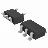
QS5U13TR Rohm Semiconductor, QS5U13TR Datasheet - Page 4

QS5U13TR
Manufacturer Part Number
QS5U13TR
Description
MOSFET N-CH 30V 2A TSMT5
Manufacturer
Rohm Semiconductor
Datasheet
1.QS5U13TR.pdf
(5 pages)
Specifications of QS5U13TR
Fet Type
MOSFET N-Channel, Metal Oxide
Fet Feature
Diode (Isolated)
Rds On (max) @ Id, Vgs
100 mOhm @ 2A, 4.5V
Drain To Source Voltage (vdss)
30V
Current - Continuous Drain (id) @ 25° C
2A
Vgs(th) (max) @ Id
1.5V @ 1mA
Gate Charge (qg) @ Vgs
3.9nC @ 4.5V
Input Capacitance (ciss) @ Vds
175pF @ 10V
Power - Max
900mW
Mounting Type
Surface Mount
Package / Case
TSMT5
Configuration
Single
Transistor Polarity
N-Channel
Resistance Drain-source Rds (on)
0.1 Ohm @ 4.5 V
Drain-source Breakdown Voltage
30 V
Gate-source Breakdown Voltage
12 V
Continuous Drain Current
2 A
Power Dissipation
1250 mW
Maximum Operating Temperature
+ 150 C
Mounting Style
SMD/SMT
Minimum Operating Temperature
- 50 C
Lead Free Status / RoHS Status
Lead free / RoHS Compliant
Transistors
Measurement circuits
6
5
4
3
2
1
0
Fig.10 Dynamic Input Characteristics
0
Fig.15 Gate Charge Measurement Circuit
Fig.13 Switching Time Measurement Circuit
Ta=25°C
V
I
R
Pulsed
I
D
G(Const.)
DD
=2A
G
=10Ω
TOTAL GATE CHARGE : Qg (nC)
=15V
R
R
1
G
G
V
V
GS
GS
2
D.U.T.
D.U.T.
I
I
D
D
3
R
R
V
V
L
L
DD
DD
V
V
DS
DS
1000
100
0.1
10
1
0
Fig.11 Forward Current
125°C
75°C
25°C
−25°C
FORWARD VOLTAGE : V
0.1
vs. Forward Voltage
0.2
0.3
0.4
F
(V)
V
V
0.5
GS
DS
V
t
d(on)
Fig.14 Switching Waveforms
GS
V
Fig.16 Gate Charge Waveform
10%
0.0001
t
G
50%
0.001
on
Q
0.01
100
0.1
10
gs
10%
t
1
r
0
Fig.12 Reverse Current
Pulse Width
Q
90%
REVERSE VOLTAGE : V
gd
Q
10
g
vs. Reverse Voltage
Rev.A
90%
20
t
d(off)
QS5U13
Charge
t
off
30
t
f
R
50%
125°C
75°C
25°C
−25°C
(V)
10%
90%
4/4
4
0


