STP20NM60FP STMicroelectronics, STP20NM60FP Datasheet
STP20NM60FP
Specifications of STP20NM60FP
Available stocks


Related parts for STP20NM60FP


STP20NM60FP Summary of contents
Page 1
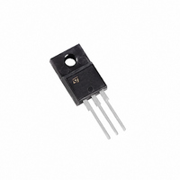
... APPLICATIONS The MDmesh™ family is very suitable for increas- ing power density of high voltage converters allow- ing system miniaturization and higher efficiencies. Table 2: Order Codes SALES TYPE STP20NM60 STP20NM60FP STB20NM60T4 STB20NM60-1 STW20NM60 February 2005 STB20NM60 - STB20NM60-1 Figure 1: Package R ...
Page 2
... STP20NM60 - STP20NM60FP - STB20NM60 - STW20NM60 - STB20NM60-1 Table 3: Absolute Maximum ratings Symbol V Drain-source Voltage ( Drain-gate Voltage (R DGR V Gate- source Voltage GS I Drain Current (continuous Drain Current (continuous Drain Current (pulsed Total Dissipation at T TOT Derating Factor dv/dt (1) Peak Diode Recovery voltage slope V Insulation Winthstand Voltage (DC) ...
Page 3
... STP20NM60 - STP20NM60FP - STB20NM60 - STW20NM60 - STB20NM60-1 ELECTRICAL CHARACTERISTICS (CONTINUED) Table 7: Dynamic Symbol Parameter g (1) Forward Transconductance fs C Input Capacitance iss Output Capacitance C oss Reverse Transfer C rss Capacitance C (3) Equivalent Output oss eq. Capacitance t Turn-on Delay Time d(on) Rise Time t r Turn-off Delay Time ...
Page 4
... STP20NM60 - STP20NM60FP - STB20NM60 - STW20NM60 - STB20NM60-1 Figure 3: Safe Operating Area for TO-220/ D²PAK/I²PAK Figure 4: Safe Operating Area for TO-220FP Figure 5: Safe Operating Area for TO-247 4/15 Figure 6: Thermal Impedance for TO-220/ D²PAK/I²PAK Figure 7: Thermal Impedance for TO-220FP Figure 8: Thermal Impedance for TO-247 ...
Page 5
... STP20NM60 - STP20NM60FP - STB20NM60 - STW20NM60 - STB20NM60-1 Figure 9: Output Characteristics Figure 10: Transconductance Figure 11: Transfer Characteristics Figure 12: Gate Charge vs Gate-source Voltage Figure 13: Normalized Gate Threshold Voltage vs Temp. Figure 14: Static Drain-source On Resistance 5/15 ...
Page 6
... STP20NM60 - STP20NM60FP - STB20NM60 - STW20NM60 - STB20NM60-1 Figure 15: Capacitance Variations Figure 16: Normalized On Resistance vs Tem- perature 6/15 Figure 17: Source-drain Diode Forward Char- acteristics ...
Page 7
... STP20NM60 - STP20NM60FP - STB20NM60 - STW20NM60 - STB20NM60-1 Figure 18: Unclamped Inductive Load Test Cir- cuit Figure 19: Switching Times Test Circuit For Resistive Load Figure 20: Test Circuit For Inductive Load Switching and Diode Recovery Times Figure 21: Unclamped Inductive Wafeform Figure 22: Gate Charge Test Circuit 7/15 ...
Page 8
... STP20NM60 - STP20NM60FP - STB20NM60 - STW20NM60 - STB20NM60-1 DIM. MIN. A 4.40 b 0.61 b1 1.15 c 0.49 D 15. 2.40 e1 4.95 F 1.23 H1 6. 3.50 L20 L30 øP 3.75 Q 2.65 8/15 TO-220 MECHANICAL DATA mm. TYP MAX. MIN. 4.60 0.173 0.88 0.024 1.70 0.045 0.70 0.019 15.75 0.60 10.40 ...
Page 9
... STP20NM60 - STP20NM60FP - STB20NM60 - STW20NM60 - STB20NM60-1 TO-220FP MECHANICAL DATA mm. DIM. MIN. TYP A 4.4 B 2.5 D 2.5 E 0.45 F 0.75 F1 1.15 F2 1.15 G 4. 28.6 L4 9.8 L5 2 Ø inch MAX. MIN. TYP. 4.6 0.173 2.7 0.098 2.75 0.098 0.7 0.017 1 0.030 1.7 0.045 1.7 ...
Page 10
... STP20NM60 - STP20NM60FP - STB20NM60 - STW20NM60 - STB20NM60-1 DIM. MIN. A 4.32 A1 0.00 b 0.71 b2 1.15 c 0.46 c2 1.22 D 8.89 D1 8.01 E 10. 13.10 L 1.30 L1 1.15 L2 1.27 L4 2.70 V2 0° 10/15 2 TO-263 (D PAK) MECHANICAL DATA mm. TYP MAX. MIN. 4.57 0.178 0.25 0.00 0.91 0.028 1.40 0.045 0.61 0.018 1 ...
Page 11
... STP20NM60 - STP20NM60FP - STB20NM60 - STW20NM60 - STB20NM60-1 TO-262 (I mm. DIM. MIN. TYP A 4.40 A1 2.40 b 0.61 b1 1.14 c 0.49 c2 1.23 D 8.95 e 2. 3.50 L2 1.27 2 PAK) MECHANICAL DATA inch MAX. MIN. TYP. 4.60 0.173 2.72 0.094 0.88 0.024 1.70 0.044 0.70 0.019 1.32 0.048 9.35 ...
Page 12
... STP20NM60 - STP20NM60FP - STB20NM60 - STW20NM60 - STB20NM60 PAK FOOTPRINT TAPE AND REEL SHIPMENT (suffix ”T4”)* TAPE MECHANICAL DATA mm DIM. MIN. MAX. A0 10.5 10.7 B0 15.7 15.9 D 1.5 1.6 D1 1.59 1.61 E 1.65 1.85 F 11.4 11.6 K0 4.8 5.0 P0 3.9 4.1 P1 11.9 12.1 P2 1.9 2 0.25 0.35 0.0098 0.0137 W 23 ...
Page 13
... STP20NM60 - STP20NM60FP - STB20NM60 - STW20NM60 - STB20NM60-1 TO-247 MECHANICAL DATA mm. DIM. MIN. TYP A 4.85 A1 2.20 b 1.0 b1 2.0 b2 3.0 c 0.40 D 19.85 E 15.45 e 5.45 L 14.20 L1 3.70 L2 18.50 øP 3.55 øR 4.50 S 5.50 inch MAX. MIN. TYP. 5.15 0.19 2.60 0.086 1.40 0.039 2.40 0.079 3.40 ...
Page 14
... STP20NM60 - STP20NM60FP - STB20NM60 - STW20NM60 - STB20NM60-1 Table 9: Revision History Date Revision 26-Jul-2004 1 17-Feb-2005 2 14/15 Description of Changes First Release Insert the TO-247 package ...
Page 15
... STP20NM60 - STP20NM60FP - STB20NM60 - STW20NM60 - STB20NM60-1 Information furnished is believed to be accurate and reliable. However, STMicroelectronics assumes no responsibility for the consequences of use of such information nor for any infringement of patents or other rights of third parties which may result from its use. No license is granted by implication or otherwise under any patent or patent rights of STMicroelectronics. Specifications mentioned in this publication are subject to change without notice ...