STW34NB20 STMicroelectronics, STW34NB20 Datasheet
STW34NB20
Specifications of STW34NB20
Available stocks


Related parts for STW34NB20


STW34NB20 Summary of contents
Page 1
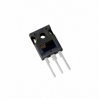
... HIGH CURRENT, HIGH SPEED SWITCHING ■ Table 2. Order Codes Part Number STW34NB20 April 2004 N-CHANNEL 200V - 0.062 Ω - 34A TO-247 Figure 1. Package R I DS(on Figure 2. Internal Schematic Diagram Marking Package TO-247 W34NB20 STW34NB20 PowerMESH™ MOSFET TO-247 Packaging TUBE REV. 2 1/10 ...
Page 2
... STW34NB20 Table 3. Absolute Maximum Ratings Symbol V Drain-source Voltage ( Drain- gate Voltage (R DGR V Gate-source Voltage GS I Drain Current (cont Drain Current (cont (1) Drain Current (pulsed Total Dissipation at T tot Derating Factor T Storage Temperature stg T Max. Operating Junction Temperature j Note: 1. Pulse width limited by safe operating area Table 4 ...
Page 3
... Test Conditions = 4.7 Ω 100 (see test circuit, Figure 16 160 Test Conditions = 4.7 Ω 160 (see test circuit, Figure 18) GS STW34NB20 Min. Typ. Max. Unit 200 V µA 1 µA 10 ± 100 nA Min. Typ. Max. Unit Ω 0.062 0.075 Min. Typ. Max. Unit 8 ...
Page 4
... STW34NB20 Table 11. Source Drain Diode Symbol Parameter I Source-drain Current SD (1) Source-drain Current I SDM (pulsed) (2) Forward On Voltage Reverse Recovery Time rr Q Reverse RecoveryCharge rr I Reverse RecoveryCharge RRAM Note: 1. Pulse width limited by safe operating area 2. Pulsed: Pulse duration = 300 µs, duty cycle 1.5 % Figure 3 ...
Page 5
... Figure 7. Transconductance Figure 9. Gate Charge vs Gate-source Voltage Figure 11. Normalized Gate Thresold Voltage vs Temperature Figure 8. Static Drain-source On Resistance Figure 10. Capacitance Variations Figure 12. Normalized On Resistance vs Temperature STW34NB20 5/10 ...
Page 6
... STW34NB20 Figure 13. Source-drain Diode Forward Characteristics 6/10 ...
Page 7
... Figure 14. Unclamped Inductive Load Test Circuit Figure 16. Switching Times Test Circuits For Resistive Load Figure 18. Test Circuit For Inductive Load Switching And Diode Recovery Times Figure 15. Unclamped Inductive Waveforms Figure 17. Gate Charge Test Circuit STW34NB20 7/10 ...
Page 8
... STW34NB20 PACKAGE MECHANICAL Table 12. TO-247 Mechanical Data Symbol Min A 4.85 A1 2.20 b 1.0 b1 2.0 b2 3.0 c 0.40 D 19.85 E 15. 14.20 L1 3.70 L2 ØP 3.55 ØR 4.50 S Figure 19. TO-247 Package Dimensions Note: Drawing is not to scale. 8/10 millimeters Typ Max 5.15 2.60 1.40 2.40 3.40 0.80 20 ...
Page 9
... REVISION HISTORY Table 13. Revision History Date Revision January-1998 1 14-Apr-2004 2 Description of Changes First Issue Stylesheet update. No content change. STW34NB20 9/10 ...
Page 10
... STW34NB20 Information furnished is believed to be accurate and reliable. However, STMicroelectronics assumes no responsibility for the consequences of use of such information nor for any infringement of patents or other rights of third parties which may result from its use. No license is granted by implication or otherwise under any patent or patent rights of STMicroelectronics. Specifications mentioned in this publication are subject to change without notice ...