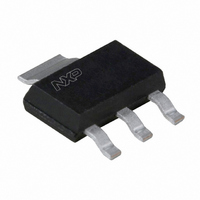
PHT6NQ10T,135 NXP Semiconductors, PHT6NQ10T,135 Datasheet - Page 3

PHT6NQ10T,135
Manufacturer Part Number
PHT6NQ10T,135
Description
MOSFET N-CH 100V 6.5A SOT223
Manufacturer
NXP Semiconductors
Series
TrenchMOS™r
Datasheet
1.PHT6NQ10T135.pdf
(7 pages)
Specifications of PHT6NQ10T,135
Package / Case
SOT-223 (3 leads + Tab), SC-73, TO-261
Fet Type
MOSFET N-Channel, Metal Oxide
Fet Feature
Standard
Rds On (max) @ Id, Vgs
90 mOhm @ 3A, 10V
Drain To Source Voltage (vdss)
100V
Current - Continuous Drain (id) @ 25° C
6.5A
Vgs(th) (max) @ Id
4V @ 1mA
Gate Charge (qg) @ Vgs
21nC @ 10V
Input Capacitance (ciss) @ Vds
633pF @ 25V
Power - Max
8.3W
Mounting Type
Surface Mount
Minimum Operating Temperature
- 65 C
Configuration
Single Dual Drain
Transistor Polarity
N-Channel
Resistance Drain-source Rds (on)
0.09 Ohm @ 10 V
Drain-source Breakdown Voltage
100 V
Gate-source Breakdown Voltage
+/- 20 V
Continuous Drain Current
3 A
Power Dissipation
1800 mW
Maximum Operating Temperature
+ 150 C
Mounting Style
SMD/SMT
Lead Free Status / RoHS Status
Lead free / RoHS Compliant
Lead Free Status / RoHS Status
Lead free / RoHS Compliant, Lead free / RoHS Compliant
Other names
934055876135
PHT6NQ10T /T3
PHT6NQ10T /T3
PHT6NQ10T /T3
PHT6NQ10T /T3
Available stocks
Company
Part Number
Manufacturer
Quantity
Price
Part Number:
PHT6NQ10T,135
Manufacturer:
NEXPERIA/安世
Quantity:
20 000
Philips Semiconductors
August 1999
N-channel TrenchMOS
100
100
0.01
100
90
80
70
60
50
40
30
20
10
90
80
70
60
50
40
30
20
10
0.1
10
0
0
I
1
Fig.2. Normalised continuous drain current.
D
0
0
1
Normalised Current Derating, ID (%)
& I
Normalised Power Derating, PD (%)
Peak Pulsed Drain Current, IDM (A)
RDS(on) = VDS/ ID
Fig.1. Normalised power dissipation.
ID% = 100 I
DM
= f(V
25
25
PD% = 100 P
Fig.3. Safe operating area
Solder Point temperature, Tsp (C)
Solder Point temperature, Tsp (C)
DS
Drain-Source Voltage, VDS (V)
D.C.
); I
D
10
50
50
/I
DM
D 25 ˚C
single pulse; parameter t
D
/P
= f(T
75
75
D 25 ˚C
sp
); V
100
100
= f(T
100
tp = 10 us
100 us
100 ms
1 ms
10 ms
transistor
GS
sp
)
10 V
125
125
1000
p
150
150
3
0.01
6
5
4
3
2
1
0
0.18
0.16
0.14
0.12
0.08
0.06
0.04
0.02
Fig.5. Typical output characteristics, T
100
0.1
0.2
0.1
Fig.6. Typical on-state resistance, T
10
0
1
1E-06
0
Drain Current, ID (A)
VGS = 10V
0
Drain-Source On Resistance, RDS(on) (Ohms)
6 V
Transient thermal impedance, Zth j-sp (K/W)
0.05
8 V
0.2
D = 0.5
0.2
Fig.4. Transient thermal impedance.
Tj = 25 C
4.6V
0.02
0.1
single pulse
1E-05
Z
0.4
th j-sp
1
1E-04
Drain-Source Voltage, VDS (V)
0.6
= f(t); parameter D = t
4.8V
Drain Current, ID (A)
5.4 V
2
R
Pulse width, tp (s)
0.8
I
DS(ON)
D
1E-03
= f(V
Tj = 25 C
1
3
= f(I
1E-02
DS
5 V
1.2
)
D
)
P
Product specification
D
4
1E-01
1.4
PHT6NQ10T
tp
5.2 V
p
5.2 V
T
1.6
/T
VGS = 10V
1E+00
j
D = tp/T
5
j
= 25 ˚C .
= 25 ˚C .
5.4 V
1.8
6V
4.8 V
4.6 V
4.4 V
Rev 1.000
5 V
8 V
1E+01
6
2


