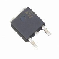
STD5N20T4 STMicroelectronics, STD5N20T4 Datasheet - Page 3

STD5N20T4
Manufacturer Part Number
STD5N20T4
Description
MOSFET N-CH 200V 5A DPAK
Manufacturer
STMicroelectronics
Series
MESH OVERLAY™r
Datasheet
1.STD5N20T4.pdf
(8 pages)
Specifications of STD5N20T4
Fet Type
MOSFET N-Channel, Metal Oxide
Fet Feature
Standard
Rds On (max) @ Id, Vgs
800 mOhm @ 2.5A, 10V
Drain To Source Voltage (vdss)
200V
Current - Continuous Drain (id) @ 25° C
5A
Vgs(th) (max) @ Id
4V @ 250µA
Gate Charge (qg) @ Vgs
27nC @ 10V
Input Capacitance (ciss) @ Vds
350pF @ 25V
Power - Max
45W
Mounting Type
Surface Mount
Package / Case
DPak, TO-252 (2 leads+tab), SC-63
Configuration
Single
Transistor Polarity
N-Channel
Resistance Drain-source Rds (on)
0.8 Ohm @ 10 V
Forward Transconductance Gfs (max / Min)
4 S
Drain-source Breakdown Voltage
200 V
Gate-source Breakdown Voltage
+/- 20 V
Continuous Drain Current
5 A
Power Dissipation
45000 mW
Maximum Operating Temperature
+ 150 C
Mounting Style
SMD/SMT
Minimum Operating Temperature
- 65 C
Continuous Drain Current Id
2.5A
Drain Source Voltage Vds
200V
On Resistance Rds(on)
700mohm
Rds(on) Test Voltage Vgs
10V
Threshold Voltage Vgs Typ
3V
Rohs Compliant
Yes
Lead Free Status / RoHS Status
Lead free / RoHS Compliant
Other names
497-6563-2
STD5N20T4
STD5N20T4
Available stocks
Company
Part Number
Manufacturer
Quantity
Price
Company:
Part Number:
STD5N20T4
Manufacturer:
ST
Quantity:
12 500
Part Number:
STD5N20T4
Manufacturer:
ST
Quantity:
20 000
ELECTRICAL CHARACTERISTICS (CONTINUED)
SWITCHING ON
SWITCHING OFF
SOURCE DRAIN DIODE
Note: 1. Pulsed: Pulse duration = 300 µs, duty cycle 1.5 %.
Safe Operating Area
Symbol
Symbol
Symbol
I
V
SDM
t
t
I
SD
r(Voff)
d(on)
Q
Q
RRM
I
2. Pulse width limited by safe operating area.
Q
Q
SD
t
t
t
t
rr
gs
gd
c
r
f
rr
g
(1)
(2)
Turn-on Delay Time
Rise Time
Total Gate Charge
Gate-Source Charge
Gate-Drain Charge
Source-drain Current
Source-drain Current (pulsed)
Forward On Voltage
Reverse Recovery Time
Reverse Recovery Charge
Reverse Recovery Current
Off-voltage Rise Time
Fall Time
Cross-over Time
Parameter
Parameter
Parameter
V
R
(see test circuit, Figure 3)
V
V
I
I
V
(see test circuit, Figure 5)
V
R
(see test circuit, Figure 5)
SD
SD
DD
DD
GS
DD
G
DD
G
= 4.7
= 4.7
= 6 A, V
=6 A, di/dt = 100A/µs
= 100 V, I
= 160V, I
= 10V
= 100V, T
= 160V, I
Test Conditions
Test Conditions
Test Conditions
V
V
GS
GS
GS
D
D
D
j
= 0
= 150°C
Thermal Impedance
= 6 A,
= 6 A,
= 10 V
= 3 A
= 10V
Min.
Min.
Min.
Typ.
Typ.
Typ.
155
700
4.5
7.5
18
30
19
40
10
65
9
Max.
Max.
Max.
1.5
27
24
6
STD5N20
Unit
Unit
Unit
nC
nC
nC
nC
ns
ns
ns
ns
ns
ns
A
A
V
A
3/8


