IRF6645TRPBF International Rectifier, IRF6645TRPBF Datasheet - Page 2
IRF6645TRPBF
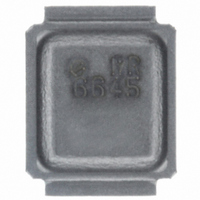
Manufacturer Part Number
IRF6645TRPBF
Description
MOSFET N-CH 100V 5.7A DIRECTFET
Manufacturer
International Rectifier
Series
HEXFET®r
Datasheet
1.IRF6645TRPBF.pdf
(10 pages)
Specifications of IRF6645TRPBF
Fet Type
MOSFET N-Channel, Metal Oxide
Fet Feature
Standard
Rds On (max) @ Id, Vgs
35 mOhm @ 5.7A, 10V
Drain To Source Voltage (vdss)
100V
Current - Continuous Drain (id) @ 25° C
5.7A
Vgs(th) (max) @ Id
4.9V @ 50µA
Gate Charge (qg) @ Vgs
20nC @ 10V
Input Capacitance (ciss) @ Vds
890pF @ 25V
Power - Max
3W
Mounting Type
Surface Mount
Package / Case
DirectFET™ Isometric SJ
Transistor Polarity
N-Channel
Drain-source Breakdown Voltage
100 V
Gate-source Breakdown Voltage
20 V
Continuous Drain Current
5.7 A
Power Dissipation
42 W
Gate Charge Qg
14 nC
For Use With
IRAUDAMP5 - BOARD DEMO IRS2092S/IRF6645IRAUDAMP4 - KIT 2CH 120W HALF BRDG AUDIO AMP
Lead Free Status / RoHS Status
Lead free / RoHS Compliant
Other names
IRF6645TRPBFTR
Available stocks
Company
Part Number
Manufacturer
Quantity
Price

Part Number:
IRF6645TRPBF
Manufacturer:
IR
Quantity:
20 000


Notes:
…
‡
IRF6645PbF
Electrical Characteristic @ T
BV
∆ΒV
R
V
∆V
I
I
gfs
Q
Q
Q
R
t
t
t
t
C
C
C
C
C
Diode Characteristics
I
I
V
t
Q
DSS
GSS
d(on)
r
d(off)
f
S
SM
rr
GS(th)
SD
DS(on)
Q
Q
Q
Q
G
iss
oss
rss
oss
oss
g
sw
oss
rr
Repetitive rating; pulse width limited by max. junction temperature.
Pulse width ≤ 400µs; duty cycle ≤ 2%.
2
GS(th)
DSS
gs1
gs2
gd
godr
DSS
/∆T
/∆T
J
J
Drain-to-Source Breakdown Voltage
Breakdown Voltage Temp. Coefficient
Static Drain-to-Source On-Resistance
Gate Threshold Voltage
Gate Threshold Voltage Coefficient
Drain-to-Source Leakage Current
Gate-to-Source Forward Leakage
Gate-to-Source Reverse Leakage
Forward Transconductance
Total Gate Charge
Pre-Vth Gate-to-Source Charge
Post-Vth Gate-to-Source Charge
Gate-to-Drain Charge
Gate Charge Overdrive
Switch Charge (Q
Output Charge
Gate Resistance
Turn-On Delay Time
Rise Time
Turn-Off Delay Time
Fall Time
Input Capacitance
Output Capacitance
Reverse Transfer Capacitance
Output Capacitance
Output Capacitance
Continuous Source Current
(Body Diode)
Pulsed Source Current
(Body Diode) g
Diode Forward Voltage
Reverse Recovery Time
Reverse Recovery Charge
Parameter
Parameter
gs2
J
+ Q
= 25°C (unless otherwise specified)
gd
)
Min.
Min.
100
–––
–––
–––
–––
–––
–––
–––
–––
–––
–––
–––
–––
–––
–––
–––
–––
–––
–––
–––
–––
–––
–––
–––
–––
–––
–––
–––
–––
–––
3.0
7.4
Typ.
Typ.
0.12
–––
–––
–––
–––
–––
–––
–––
890
180
870
100
–––
–––
–––
-12
3.1
0.8
4.8
5.3
5.6
7.2
1.0
9.2
5.0
5.1
28
14
18
40
31
40
Max. Units
Max. Units
-100
–––
–––
–––
250
100
–––
–––
–––
–––
–––
–––
–––
–––
–––
–––
–––
–––
–––
–––
–––
–––
4.9
7.2
1.3
35
20
20
25
45
47
60
mV/°C
V/°C
mΩ
nC
nC
nC
µA
nA
pF
ns
ns
V
V
S
Ω
A
V
V
Reference to 25°C, I
V
V
V
V
V
V
V
V
V
I
See Fig. 15
V
V
I
R
V
V
ƒ = 1.0MHz
V
V
MOSFET symbol
showing the
integral reverse
p-n junction diode.
T
T
di/dt = 100A/µs c
D
D
J
J
GS
GS
DS
DS
DS
GS
GS
DS
DS
GS
DS
DD
GS
DS
GS
GS
G
= 3.4A
= 3.4A
=6.2Ω
= 25°C, I
= 25°C, I
= V
= 100V, V
= 80V, V
= 10V, I
= 50V
= 16V, V
= 25V
= 0V, I
= 10V, I
= 20V
= -20V
= 10V
= 50V, V
= 0V
= 0V, V
= 0V, V
GS
, I
Conditions
Conditions
D
S
F
D
DS
DS
D
D
= 250µA
GS
GS
GS
= 3.4A, V
= 3.4A, V
= 50µA
= 5.7A i
= 3.4A
GS
= 1.0V, f=1.0MHz
= 80V, f=1.0MHz
= 0V, T
= 0V
= 10V i
= 0V
www.irf.com
D
= 1mA
GS
DD
J
G
= 125°C
= 0V i
= 50V
S
D
Related parts for IRF6645TRPBF
Image
Part Number
Description
Manufacturer
Datasheet
Request
R

Part Number:
Description:
MOSFET N-CH 100V DIRECTFET-SJ
Manufacturer:
International Rectifier
Datasheet:

Part Number:
Description:
SCHOTTKY RECTIFIER
Manufacturer:
International Rectifier Corp.
Datasheet:
Part Number:
Description:
SCHOTTKY RECTIFIER
Manufacturer:
International Rectifier Corp.
Datasheet:
Part Number:
Description:
SCHOTTKY RECTIFIER
Manufacturer:
International Rectifier Corp.
Datasheet:
Part Number:
Description:
SCHOTTKY RECTIFIER
Manufacturer:
International Rectifier Corp.
Datasheet:
Part Number:
Description:
SCHOTTKY RECTIFIER
Manufacturer:
International Rectifier Corp.
Datasheet:
Part Number:
Description:
SCHOTTKY RECTIFIER
Manufacturer:
International Rectifier Corp.
Datasheet:
Part Number:
Description:
SCHOTTKY RECTIFIER
Manufacturer:
International Rectifier Corp.
Datasheet:
Part Number:
Description:
SCHOTTKY RECTIFIER
Manufacturer:
International Rectifier Corp.
Datasheet:
Part Number:
Description:
SCHOTTKY RECTIFIER
Manufacturer:
International Rectifier Corp.
Datasheet:
Part Number:
Description:
SCHOTTKY RECTIFIER
Manufacturer:
International Rectifier Corp.
Datasheet:
Part Number:
Description:
SCHOTTKY RECTIFIER
Manufacturer:
International Rectifier Corp.
Datasheet:
Part Number:
Description:
SCHOTTKY RECTIFIER
Manufacturer:
International Rectifier Corp.
Datasheet:
Part Number:
Description:
SCHOTTKY RECTIFIER
Manufacturer:
International Rectifier Corp.
Datasheet:
Part Number:
Description:
SCHOTTKY RECTIFIER
Manufacturer:
International Rectifier Corp.
Datasheet: