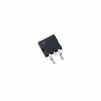
STB9NK60ZT4 STMicroelectronics, STB9NK60ZT4 Datasheet - Page 2

STB9NK60ZT4
Manufacturer Part Number
STB9NK60ZT4
Description
MOSFET N-CH 600V 7A D2PAK
Manufacturer
STMicroelectronics
Series
SuperMESH™r
Datasheet
1.STB9NK60ZT4.pdf
(13 pages)
Specifications of STB9NK60ZT4
Fet Type
MOSFET N-Channel, Metal Oxide
Fet Feature
Standard
Rds On (max) @ Id, Vgs
950 mOhm @ 3.5A, 10V
Drain To Source Voltage (vdss)
600V
Current - Continuous Drain (id) @ 25° C
7A
Vgs(th) (max) @ Id
4.5V @ 100µA
Gate Charge (qg) @ Vgs
53nC @ 10V
Input Capacitance (ciss) @ Vds
1110pF @ 25V
Power - Max
125W
Mounting Type
Surface Mount
Package / Case
D²Pak, TO-263 (2 leads + tab)
Transistor Polarity
N Channel
Continuous Drain Current Id
3.5A
Drain Source Voltage Vds
600V
On Resistance Rds(on)
850mohm
Rds(on) Test Voltage Vgs
10V
Threshold Voltage Vgs Typ
3.75V
Rohs Compliant
Yes
Configuration
Single
Resistance Drain-source Rds (on)
0.95 Ohms
Forward Transconductance Gfs (max / Min)
5.3 S
Drain-source Breakdown Voltage
600 V
Gate-source Breakdown Voltage
+/- 30 V
Continuous Drain Current
7 A
Power Dissipation
125 W
Maximum Operating Temperature
+ 150 C
Mounting Style
SMD/SMT
Minimum Operating Temperature
- 55 C
Lead Free Status / RoHS Status
Lead free / RoHS Compliant
Available stocks
Company
Part Number
Manufacturer
Quantity
Price
Company:
Part Number:
STB9NK60ZT4
Manufacturer:
ST
Quantity:
25 000
Company:
Part Number:
STB9NK60ZT4
Manufacturer:
ST
Quantity:
12 500
Part Number:
STB9NK60ZT4
Manufacturer:
ST
Quantity:
20 000
STP9NK60Z / STP9NK60ZFP / STB9NK60Z / STB9NK60Z-1
ABSOLUTE MAXIMUM RATINGS
(
(1) I
(*) Limited only by maximum temperature allowed
THERMAL DATA
AVALANCHE CHARACTERISTICS
GATE-SOURCE ZENER DIODE
PROTECTION FEATURES OF GATE-TO-SOURCE ZENER DIODES
The built-in back-to-back Zener diodes have specifically been designed to enhance not only the device’s
ESD capability, but also to make them safely absorb possible voltage transients that may occasionally be
applied from gate to souce. In this respect the Zener voltage is appropriate to achieve an efficient and cost-
effective intervention to protect the device’s integrity. These integrated Zener diodes thus avoid the usage
of external components.
2/13
l
) Pulse width limited by safe operating area
V
Rthj-case
Rthj-amb
dv/dt (1)
Rthj-pcb
Symbol
Symbol
Symbol
SD
BV
ESD(G-S)
I
V
DM
P
V
V
V
E
T
I
DGR
I
I
TOT
AR
T
T
ISO
stg
GSO
DS
GS
AS
D
D
7A, di/dt 200
j
l
(
l
)
Avalanche Current, Repetitive or Not-Repetitive
(pulse width limited by T
Single Pulse Avalanche Energy
(starting T
Gate-Source Breakdown
Voltage
Thermal Resistance Junction-case Max
Thermal Resistance Junction-pcb Max
(When mounted on minimum Footprint)
Thermal Resistance Junction-ambient Max
Maximum Lead Temperature For Soldering Purpose
Drain-source Voltage (V
Drain-gate Voltage (R
Gate- source Voltage
Drain Current (continuous) at T
Drain Current (continuous) at T
Drain Current (pulsed)
Total Dissipation at T
Derating Factor
Gate source ESD(HBM-C=100pF, R=1.5K
Peak Diode Recovery voltage slope
Insulation Withstand Voltage (DC)
Operating Junction Temperature
Storage Temperature
µ
A, V
Parameter
DD
j
= 25 °C, I
V
(BR)DSS
D
Parameter
C
GS
, T
= I
= 25°C
GS
j
j
= 20 k )
max)
AR
Parameter
T
= 0)
, V
JMAX.
DD
C
C
Igs=± 1mA (Open Drain)
= 25°C
= 100°C
= 50 V)
Test Conditions
TO-220
I
D
2
2
PAK
PAK / I
TO-220 /
125
4.4
28
7
1
-
2
1
PAK
Min.
30
-55 to 150
-55 to 150
Value
62.5
4000
300
± 30
D
600
600
4.5
2
Max Value
30
PAK
235
Typ.
7
TO-220FP
4.4 (*)
28 (*)
2500
0.24
7 (*)
30
220FP
4.16
TO-
Max.
°C/W
°C/W
°C/W
W/°C
Unit
Unit
Unit
V/ns
°C
mJ
°C
°C
A
W
V
V
V
V
A
A
A
V
V


