BF1212R,215 NXP Semiconductors, BF1212R,215 Datasheet - Page 11
BF1212R,215
Manufacturer Part Number
BF1212R,215
Description
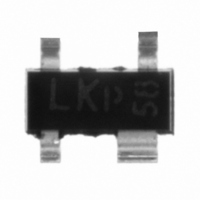
MOSFET N-CH DUAL GATE 6V SOT143R
Manufacturer
NXP Semiconductors
Datasheet
1.BF1212R215.pdf
(16 pages)
Specifications of BF1212R,215
Package / Case
SC-61B
Transistor Type
N-Channel Dual Gate
Frequency
400MHz
Gain
30dB
Voltage - Rated
6V
Current Rating
30mA
Noise Figure
0.9dB
Current - Test
12mA
Voltage - Test
5V
Configuration
Single Dual Gate
Continuous Drain Current
0.03 A
Drain-source Breakdown Voltage
6 V
Gate-source Breakdown Voltage
6 V
Maximum Operating Temperature
+ 150 C
Minimum Operating Temperature
- 65 C
Mounting Style
SMD/SMT
Power Dissipation
180 mW
Transistor Polarity
N-Channel
Application
VHF/UHF
Channel Type
N
Channel Mode
Enhancement
Drain Source Voltage (max)
6V
Power Gain (typ)@vds
35@5VdB
Noise Figure (max)
1.8dB
Package Type
SOT-143R
Pin Count
3 +Tab
Input Capacitance (typ)@vds
1.7@5V@Gate 1/1.1@5V@Gate 2pF
Output Capacitance (typ)@vds
0.9@5VpF
Reverse Capacitance (typ)
0.015@5VpF
Operating Temp Range
-65C to 150C
Mounting
Surface Mount
Number Of Elements
2
Power Dissipation (max)
180mW
Screening Level
Military
Lead Free Status / RoHS Status
Lead free / RoHS Compliant
Power - Output
-
Lead Free Status / Rohs Status
Lead free / RoHS Compliant
Other names
568-1963-2
934057518215
BF1212R
934057518215
BF1212R


NXP Semiconductors
PACKAGE OUTLINES
2003 Nov 14
Plastic surface-mounted package; 4 leads
N-channel dual-gate MOS-FETs
DIMENSIONS (mm are the original dimensions)
UNIT
mm
VERSION
OUTLINE
SOT143B
1.1
0.9
A
max
0.1
A 1
4
1
y
0.48
0.38
b p
b 1
IEC
0.88
0.78
b 1
D
e
0.15
0.09
e 1
c
JEDEC
3.0
2.8
D
REFERENCES
b p
0
1.4
1.2
E
3
2
1.9
w
e
B
JEITA
scale
M
11
1
B
1.7
e 1
v
M
H E
2.5
2.1
BF1212; BF1212R; BF1212WR
2 mm
A
A
0.45
0.15
L p
A 1
0.55
0.45
Q
detail X
PROJECTION
0.2
EUROPEAN
v
H E
E
0.1
w
Q
L p
Product specification
0.1
y
A
ISSUE DATE
04-11-16
06-03-16
c
SOT143B
X
Related parts for BF1212R,215
Image
Part Number
Description
Manufacturer
Datasheet
Request
R

Part Number:
Description:
Enhancement type N-channel Field-Effect Transistor in a plastic SOT143B package
Manufacturer:
NXP Semiconductors
Datasheet:

Part Number:
Description:
Enhancement type N-channel Field-Effect Transistor in a plastic SOT143B package
Manufacturer:
NXP Semiconductors
Datasheet:

Part Number:
Description:
MOSFET N-CH DUAL GATE 6V SOT143B
Manufacturer:
NXP Semiconductors
Datasheet:

Part Number:
Description:
Sensor Mounting Bracket
Manufacturer:
PEPPERL & FUCHS
Datasheet:
Part Number:
Description:
Cables/Accessories
Manufacturer:
PEPPERL & FUCHS
Datasheet:

Part Number:
Description:
NXP Semiconductors designed the LPC2420/2460 microcontroller around a 16-bit/32-bitARM7TDMI-S CPU core with real-time debug interfaces that include both JTAG andembedded trace
Manufacturer:
NXP Semiconductors
Datasheet:

Part Number:
Description:
NXP Semiconductors designed the LPC2458 microcontroller around a 16-bit/32-bitARM7TDMI-S CPU core with real-time debug interfaces that include both JTAG andembedded trace
Manufacturer:
NXP Semiconductors
Datasheet:
Part Number:
Description:
NXP Semiconductors designed the LPC2468 microcontroller around a 16-bit/32-bitARM7TDMI-S CPU core with real-time debug interfaces that include both JTAG andembedded trace
Manufacturer:
NXP Semiconductors
Datasheet:
Part Number:
Description:
NXP Semiconductors designed the LPC2470 microcontroller, powered by theARM7TDMI-S core, to be a highly integrated microcontroller for a wide range ofapplications that require advanced communications and high quality graphic displays
Manufacturer:
NXP Semiconductors
Datasheet:
Part Number:
Description:
NXP Semiconductors designed the LPC2478 microcontroller, powered by theARM7TDMI-S core, to be a highly integrated microcontroller for a wide range ofapplications that require advanced communications and high quality graphic displays
Manufacturer:
NXP Semiconductors
Datasheet:
Part Number:
Description:
The Philips Semiconductors XA (eXtended Architecture) family of 16-bit single-chip microcontrollers is powerful enough to easily handle the requirements of high performance embedded applications, yet inexpensive enough to compete in the market for hi
Manufacturer:
NXP Semiconductors
Datasheet:
Part Number:
Description:
The XA-S3 device is a member of Philips Semiconductors? XA(eXtended Architecture) family of high performance 16-bitsingle-chip microcontrollers
Manufacturer:
NXP Semiconductors
Datasheet:

Part Number:
Description:
The NXP BlueStreak LH75401/LH75411 family consists of two low-cost 16/32-bit System-on-Chip (SoC) devices
Manufacturer:
NXP Semiconductors
Datasheet:
Part Number:
Description:
The NXP LPC3130/3131 combine an 180 MHz ARM926EJ-S CPU core, high-speed USB2
Manufacturer:
NXP Semiconductors
Datasheet: