BLF861A,112 NXP Semiconductors, BLF861A,112 Datasheet - Page 3
BLF861A,112
Manufacturer Part Number
BLF861A,112
Description
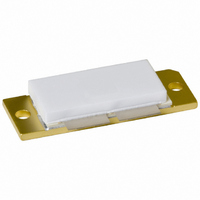
TRANSISTOR RF LDMOS SOT540A
Manufacturer
NXP Semiconductors
Datasheet
1.BLF861A112.pdf
(16 pages)
Specifications of BLF861A,112
Package / Case
SOT540A
Transistor Type
LDMOS
Frequency
860MHz
Gain
14.5dB
Voltage - Rated
65V
Current Rating
18A
Current - Test
1A
Voltage - Test
32V
Power - Output
150W
Minimum Operating Temperature
- 65 C
Mounting Style
SMD/SMT
Resistance Drain-source Rds (on)
0.16 Ohm (Typ)
Transistor Polarity
N-Channel
Configuration
Single Dual Drain Dual Gate
Drain-source Breakdown Voltage
65 V
Gate-source Breakdown Voltage
+/- 15 V
Continuous Drain Current
18 A
Power Dissipation
318000 mW
Maximum Operating Temperature
+ 200 C
Application
UHF
Channel Type
N
Channel Mode
Enhancement
Drain Source Voltage (max)
65V
Output Power (max)
150W
Power Gain (typ)@vds
14.5@32V/14(Min)@32VdB
Frequency (max)
860MHz
Package Type
LDMOST
Pin Count
5
Forward Transconductance (typ)
4S
Drain Source Resistance (max)
160(Typ)mohm
Input Capacitance (typ)@vds
82@32VpF
Output Capacitance (typ)@vds
40@32VpF
Reverse Capacitance (typ)
6@32VpF
Operating Temp Range
-65C to 200C
Drain Efficiency (typ)
50%
Mounting
Screw
Mode Of Operation
2-Tone Class-AB/CW Class-AB/PAL BG Class-AB
Number Of Elements
1
Power Dissipation (max)
318000mW
Vswr (max)
10
Screening Level
Military
Lead Free Status / RoHS Status
Lead free / RoHS Compliant
Noise Figure
-
Lead Free Status / Rohs Status
Lead free / RoHS Compliant
Other names
568-2407
934056499112
BLF861A
BLF861A
934056499112
BLF861A
BLF861A
Available stocks
Company
Part Number
Manufacturer
Quantity
Price

Part Number:
BLF861A,112
Manufacturer:
NXP/恩智浦
Quantity:
20 000


Philips Semiconductors
THERMAL CHARACTERISTICS
CHARACTERISTICS
T
Note
1. Capacitance values without internal matching.
2001 Feb 09
R
R
V
V
I
I
I
g
R
C
C
C
handbook, halfpage
j
DSS
DSX
GSS
fs
SYMBOL
SYMBOL
(BR)DSS
GSth
th j-mb
th mb-h
= 25 C; per section; unless otherwise specified.
DSon
iss
oss
rss
UHF power LDMOS transistor
V
Fig.2
GS
C oss
(pF)
100
= 0; f = 1 MHz; T
80
60
40
20
0
0
Output capacitance as a function of
drain-source voltage; typical values per
section.
thermal resistance from junction to mounting base
thermal resistance from mounting base to heatsink
drain-source breakdown voltage
gate-source threshold voltage
drain-source leakage current
drain cut-off current
gate leakage current
forward transconductance
drain-source on-state resistance
input capacitance
output capacitance
feedback capacitance
10
j
= 25 C.
PARAMETER
20
30
PARAMETER
40
V DS (V)
MLD510
50
V
V
V
V
V
V
V
V
V
V
GS
DS
GS
GS
GS
DS
GS
GS
GS
GS
= 0; I
= 10 V; I
= 0; V
= V
= 15 V; V
= 10 V; I
= V
= 0; V
= 0; V
= 0; V
GSth
GSth
3
D
CONDITIONS
DS
DS
DS
DS
= 1.5 mA
+ 9 V; V
+ 9 V; I
D
D
= 32 V
= 32 V; f = 1 MHz
= 32 V; f = 1 MHz
= 32 V; f = 1 MHz
= 150 mA
= 4 A
DS
T
= 0
mb
D
DS
= 4 A
= 25 C; P
= 10 V
CONDITIONS
(1)
(1)
(1)
tot
= 318 W
65
4
18
MIN.
4
160
82
40
6
TYP.
Product specification
VALUE
0.55
0.2
BLF861A
5.5
2.2
25
MAX.
UNIT
K/W
K/W
V
V
A
nA
S
m
pF
pF
pF
UNIT
A
Related parts for BLF861A,112
Image
Part Number
Description
Manufacturer
Datasheet
Request
R

Part Number:
Description:
Silicon N-channel enhancement mode lateral D-MOS push-pull transistor in a SOT540A package with ceramic cap
Manufacturer:
NXP Semiconductors
Datasheet:

Part Number:
Description:
Uhf Power Ldmos Transistor
Manufacturer:
NXP Semiconductors
Datasheet:
Part Number:
Description:
NXP Semiconductors designed the LPC2420/2460 microcontroller around a 16-bit/32-bitARM7TDMI-S CPU core with real-time debug interfaces that include both JTAG andembedded trace
Manufacturer:
NXP Semiconductors
Datasheet:

Part Number:
Description:
NXP Semiconductors designed the LPC2458 microcontroller around a 16-bit/32-bitARM7TDMI-S CPU core with real-time debug interfaces that include both JTAG andembedded trace
Manufacturer:
NXP Semiconductors
Datasheet:
Part Number:
Description:
NXP Semiconductors designed the LPC2468 microcontroller around a 16-bit/32-bitARM7TDMI-S CPU core with real-time debug interfaces that include both JTAG andembedded trace
Manufacturer:
NXP Semiconductors
Datasheet:
Part Number:
Description:
NXP Semiconductors designed the LPC2470 microcontroller, powered by theARM7TDMI-S core, to be a highly integrated microcontroller for a wide range ofapplications that require advanced communications and high quality graphic displays
Manufacturer:
NXP Semiconductors
Datasheet:
Part Number:
Description:
NXP Semiconductors designed the LPC2478 microcontroller, powered by theARM7TDMI-S core, to be a highly integrated microcontroller for a wide range ofapplications that require advanced communications and high quality graphic displays
Manufacturer:
NXP Semiconductors
Datasheet:
Part Number:
Description:
The Philips Semiconductors XA (eXtended Architecture) family of 16-bit single-chip microcontrollers is powerful enough to easily handle the requirements of high performance embedded applications, yet inexpensive enough to compete in the market for hi
Manufacturer:
NXP Semiconductors
Datasheet:
Part Number:
Description:
The XA-S3 device is a member of Philips Semiconductors? XA(eXtended Architecture) family of high performance 16-bitsingle-chip microcontrollers
Manufacturer:
NXP Semiconductors
Datasheet:

Part Number:
Description:
The NXP BlueStreak LH75401/LH75411 family consists of two low-cost 16/32-bit System-on-Chip (SoC) devices
Manufacturer:
NXP Semiconductors
Datasheet:
Part Number:
Description:
The NXP LPC3130/3131 combine an 180 MHz ARM926EJ-S CPU core, high-speed USB2
Manufacturer:
NXP Semiconductors
Datasheet:
Part Number:
Description:
The NXP LPC3141 combine a 270 MHz ARM926EJ-S CPU core, High-speed USB 2
Manufacturer:
NXP Semiconductors
Part Number:
Description:
The NXP LPC3143 combine a 270 MHz ARM926EJ-S CPU core, High-speed USB 2
Manufacturer:
NXP Semiconductors

Part Number:
Description:
The NXP LPC3152 combines an 180 MHz ARM926EJ-S CPU core, High-speed USB 2
Manufacturer:
NXP Semiconductors