BLF571,112 NXP Semiconductors, BLF571,112 Datasheet
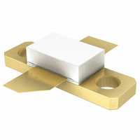
BLF571,112
Specifications of BLF571,112
934061406112
Available stocks


Related parts for BLF571,112


BLF571,112 Summary of contents
Page 1
BLF571 HF / VHF power LDMOS transistor Rev. 02 — 24 February 2009 1. Product profile 1.1 General description LDMOS RF transistor for broadcast applications and industrial applications in the HF and VHF band. Table 1. Mode ...
Page 2
... NXP Semiconductors 2. Pinning information Table 2. Pin [1] Connected to flange. 3. Ordering information Table 3. Type number BLF571 4. Limiting values Table 4. In accordance with the Absolute Maximum Rating System (IEC 60134). Symbol stg Thermal characteristics Table 5. Symbol R th(j-c) BLF571_2 Product data sheet Pinning Description drain ...
Page 3
... NXP Semiconductors 6. Characteristics Table unless otherwise specified. j Symbol Parameter V (BR)DSS V GS(th) V GSq I DSS I DSX I GSS DS(on iss C oss Table 7. Mode of operation: CW 225 MHz; RF performance at V unless otherwise specified class-AB production test circuit. Symbol BLF571_2 Product data sheet DC characteristics Conditions ...
Page 4
... NXP Semiconductors Fig 1. 6.1 Ruggedness in class-AB operation The BLF571 is capable of withstanding a load mismatch corresponding to VSWR = through all phases under the following conditions 225 MHz. 7. Application information 7.1 Impedance information Table 8. Simulated Z f MHz 225 Fig 2. BLF571_2 Product data sheet 50 C oss ...
Page 5
... NXP Semiconductors 7.2 Reliability Years (1) T (2) T (3) T (4) T (5) T (6) T (7) T (8) T (9) T (10) T (11) T Fig 3. BLF571_2 Product data sheet 5 10 (1) (2) (3) (4) (5) ( (7) (8) (9) (10) (11 0.4 TTF (0.1 % failure fraction). = 100 110 120 130 140 150 160 170 180 C ...
Page 6
... NXP Semiconductors 8. Test information 8.1 RF performance The following figures are measured in a class-AB production test circuit. 8.1.1 1-Tone (dB mA 225 MHz Fig 4. Power gain and drain efficiency as function of load power; typical values BLF571_2 Product data sheet 001aaj174 (%) (dB (W) L (1) I (2) I (3) I ...
Page 7
... NXP Semiconductors (1) P (2) P Fig 6. 8.1.2 2-Tone (dB mA 225.05 MHz. 2 Fig 7. Power gain and drain efficiency as function of peak envelope load power; typical values BLF571_2 Product data sheet (dBm mA 225 MHz 43.3 dBm (21.4 W) L(1dB dBm (25.1 W) L(3dB) Load power as function of input power; typical values ...
Page 8
... NXP Semiconductors 8.2 Test circuit Table 9. List of components All capacitors should be soldered vertically. For test circuit, see Component Description C1, C3, C4, multilayer ceramic chip capacitor 100 pF C5, C14 C2 multilayer ceramic chip capacitor multilayer ceramic chip capacitor 68 pF C7, C9 multilayer ceramic chip capacitor multilayer ceramic chip capacitor 4 ...
Page 9
... NXP Semiconductors input Fig 9. Class-AB common-source production test circuit 5.5 mm NXP BLF571 225 MHz INPUT PCB REV1 Fig 10. Component layout for class-AB production test circuit BLF571_2 Product data sheet C11 L10 L2 L11 L9 L13 L14 L12 L15 C10 9 mm Rev. 02 — 24 February 2009 ...
Page 10
... NXP Semiconductors 9. Package outline Flanged LDMOST ceramic package; 2 mounting holes; 2 leads DIMENSIONS (millimetre dimensions are derived from the original inch dimensions) UNIT 4.67 5.59 0.15 9.25 mm 3.94 5.33 0.10 9.04 0.184 0.220 0.006 0.364 inch 0.155 0.210 0.004 0.356 OUTLINE VERSION ...
Page 11
... NXP Semiconductors 10. Abbreviations Table 10. Acronym CW EDGE GSM HF LDMOS LDMOST RF TTF VHF VSWR 11. Revision history Table 11. Revision history Document ID BLF571_2 Modifications: BLF571_1 BLF571_2 Product data sheet Abbreviations Description Continuous Wave Enhanced Data rates for GSM Evolution Global System for Mobile communications ...
Page 12
... Right to make changes — NXP Semiconductors reserves the right to make changes to information published in this document, including without limitation specifications and product descriptions, at any time and without notice ...
Page 13
... NXP Semiconductors 14. Contents 1 Product profi 1.1 General description 1.2 Features . . . . . . . . . . . . . . . . . . . . . . . . . . . . . . 1 1.3 Applications . . . . . . . . . . . . . . . . . . . . . . . . . . . 1 2 Pinning information . . . . . . . . . . . . . . . . . . . . . . 2 3 Ordering information . . . . . . . . . . . . . . . . . . . . . 2 4 Limiting values Thermal characteristics Characteristics . . . . . . . . . . . . . . . . . . . . . . . . . . 3 6.1 Ruggedness in class-AB operation Application information 7.1 Impedance information . . . . . . . . . . . . . . . . . . . 4 7.2 Reliability . . . . . . . . . . . . . . . . . . . . . . . . . . . . . 5 8 Test information . . . . . . . . . . . . . . . . . . . . . . . . . 6 8.1 RF performance . . . . . . . . . . . . . . . . . . . . . . . . 6 8 ...