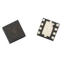
ATF-511P8-TR1 Avago Technologies US Inc., ATF-511P8-TR1 Datasheet - Page 3

ATF-511P8-TR1
Manufacturer Part Number
ATF-511P8-TR1
Description
IC PHEMT 2GHZ 4.5V 200MA 8-LPCC
Manufacturer
Avago Technologies US Inc.
Datasheet
1.ATF-511P8-BLK.pdf
(16 pages)
Specifications of ATF-511P8-TR1
Gain
14.8dB
Transistor Type
pHEMT FET
Frequency
2GHz
Voltage - Rated
7V
Current Rating
1A
Noise Figure
1.4dB
Current - Test
200mA
Voltage - Test
4.5V
Power - Output
30dBm
Package / Case
8-LPCC
Power Dissipation Pd
3W
Rf Transistor Case
LPCC
No. Of Pins
8
Frequency Max
6GHz
Noise Figure Typ
1.4dB
Frequency Min
50MHz
Continuous Drain Current Id
16.4µA
Drain Current Idss Max
200mA
Drain Source Voltage Vds
4.5V
Rohs Compliant
Yes
Lead Free Status / RoHS Status
Lead free / RoHS Compliant
Available stocks
Company
Part Number
Manufacturer
Quantity
Price
Part Number:
ATF-511P8-TR1
Manufacturer:
AVAGO/安华高
Quantity:
20 000
Company:
Part Number:
ATF-511P8-TR1G
Manufacturer:
AVAGO
Quantity:
10 000
3
ATF-511P8 Electrical Specifications
T
Symbol
Vgs
Vth
Idss
Gm
Igss
NF
G
OIP3
P1dB
PAE
ACLR
Notes:
1. Measurements obtained using production test board described in Figure 6 and PAE tested at P1dB condition.
2. I ) 2 GHz OIP3 test condition: F1 = 2.0 GHz, F2 = 2.01 GHz and Pin = -5 dBm per tone.
3. ACLR test spec is based on 3GPP TS 25.141 V5.3.1 (2002-06)
4. Use proper bias, board, heatsink and derating designs to ensure maximum channel temperature is not exceeded. See absolute maximum ratings and
Figure 6. Block diagram of the 2 GHz production test board used for NF, Gain, OIP3 , P1dB and PAE and ACLR measurements. This circuit achieves a
trade-off between optimal OIP3, P1dB and VSWR. Circuit losses have been de-embedded from actual measurements.
A
Input
II ) 900 MHz OIP3 test condition: F1 = 900 MHz, F2 = 910 MHz and Pin = -5 dBm per tone.
- Test Model 1
- Active Channels: PCCPCH + SCH + CPICH + PICH + SCCPCH + 64 DPCH (SF=128)
- Freq = 2140 MHz
- Pin = -5 dBm
- Channel Integrate Bandwidth = 3.84 MHz
application note for more details.
= 25°C, DC bias for RF parameters is Vds = 4.5V and Ids = 200 mA unless otherwise specified.
Transmission
(0.3 dB loss)
Gate Bias T
Line and
50 Ohm
Parameter and Test Condition
Operational Gate Voltage
Threshold Voltage
Saturated Drain Current
Transconductance
Gate Leakage Current
Noise Figure
Gain
Output 3
Output 1dB Compressed
Power Added Efficiency
Adjacent Channel Leakage
Power Ratio
[1]
rd
Order Intercept Point
[1,3]
[1]
Matching Circuit
[1]
Γ_ang = -164°
Γ_mag = 0.69
(1.1 dB loss)
Input
[1,2]
Vds = 4.5V, Ids = 200 mA
Vds = 4.5V, Ids = 32 mA
Vds = 4.5V, Vgs = 0V
Vds = 4.5V, Gm = ∆Idss/∆Vgs;
∆Vgs = Vgs1 – Vgs2
Vgs1 = 0.55V, Vgs2 = 0.5V
Vds = 0V, Vgs = -4.5V
f = 2 GHz
f = 900 MHz
f = 2 GHz
f = 900 MHz
f = 2 GHz
f = 900 MHz
f = 2 GHz
f = 900 MHz
f = 2 GHz
f = 900 MHz
Offset BW = 5 MHz
Offset BW = 10 MHz
DUT
Matching Circuit
Γ_ang = -163°
Γ_mag = 0.65
(0.9 dB loss)
Output
Units
V
µA
mmho
µA
dB
dB
dB
dB
dBm
dBm
dBm
dBm
%
%
dBc
dBc
V
Min.
0.25
—
—
—
-27
—
—
13.5
—
38.5
—
28.5
—
52
—
—
—
Transmission
(0.3 dB loss)
Drain Bias T
Line and
50 Ohm
Typ.
0.51
0.28
16.4
2178
-2
1.4
1.2
14.8
17.8
41.7
43
30
29.6
68.9
68.6
-58.9
-62.7
Output
Max.
0.8
—
—
—
—
—
—
16.5
—
—
—
—
—
—
—
—
—


