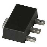
ATF-52189-BLK Avago Technologies US Inc., ATF-52189-BLK Datasheet

ATF-52189-BLK
Specifications of ATF-52189-BLK
Available stocks
Related parts for ATF-52189-BLK
ATF-52189-BLK Summary of contents
Page 1
... SOT89 package. The device is ideal as a medium-power, high-linearity amplifier. Its operating frequency range is from 50 MHz to 6 GHz. ATF-52189 is ideally suited for Cellular/PCS and WCDMA wireless infrastructure, WLAN, WLL and MMDS application, and general purpose discrete E-pHEMT amplifiers which require medium power and high linearity ...
Page 2
... ATF-52189 Absolute Maximum Ratings Symbol Parameter [2] V Drain–Source Voltage ds [2] V Gate–Source Voltage gs [2] V Gate Drain Voltage gd [2] I Drain Current ds I Gate Current gs [3] P Total Power Dissipation diss P RF Input Power in max. T Channel Temperature ch T Storage Temperature stg ATF-52189 Electrical Specifications T = 25° ...
Page 3
Symbol Parameters and Test Conditions PAE Power Added Efficiency ACLR Adjacent Channel Leakage [1,2] Power Ratio Notes: 1. Measurements at 2 GHz obtained using production test board described in Figure 1. 2. ACLR test spec is based on 3GPP TS ...
Page 4
Gamma Load and Source at Optimum OIP3 and P1dB Tuning Conditions The device’s optimum OIP3 and P1dB measurements were determined using a Maury Load Pull System at 4.5V, 200 mA quiesent bias. [1] Typical Gammas at Optimum OIP3 Freq Gamma ...
Page 5
... ATF-52189 Typical Performance Curves (at 25°C unless specified otherwise) Tuned for Optimal OIP3 4.5V, Ids = 200 mA 4.5V 15 100 150 200 250 300 350 400 Ids (mA) Figure 7. OIP3 vs. Ids and Vds at 900 MHz 4.5V 12 100 150 200 250 300 350 400 Ids (mA) Figure 10 ...
Page 6
... ATF-52189 Typical Performance Curves (at 25°C unless specified otherwise), continued Tuned for Optimal OIP3 4.5V, Ids = 200 mA. 30 Gain_3V 25 Pout_3V PAE_3V - Pin (dBm) Figure 16. Small Signal Gain/Pout/PAE vs. Pin at Vds = 3V and Frequency = 2 GHz. 30 Gain_3V 25 Pout_3V PAE_3V - Pin (dBm) Figure 19. Small Signal Gain/Pout/PAE vs. ...
Page 7
... ATF-52189 Typical Performance Curves, continued Tuned for Optimal OIP3 4.5V, Ids = 200 mA, Over Temperature and Frequency -40°C 25°C 36 80°C 34 0.5 1 1.5 2 2.5 3 3.5 4 FREQUENCY (GHz) Figure 22. OIP3 vs. Temperature and Frequency at optimum OIP3. 28 27.5 27 26.5 26 -40°C 25°C 25.5 80° ...
Page 8
... ATF-52189 Typical Performance Curves, (at 25°C unless specified otherwise) Tuned for Optimal P1dB 4.5V, Ids = 200 mA 4.5V 15 100 150 200 250 300 350 400 Ids (mA) Figure 26. OIP3 vs Ids and Vds at 900 MHz 4.5V 7 100 150 200 250 300 350 400 Ids (mA) Figure 29 ...
Page 9
... ATF-52189 Typical Performance Curves (at 25°C unless specified otherwise), continued Tuned for Optimal P1dB 4.5V, Ids = 200 mA. 35 Gain_3V 30 Pout_3V PAE_3V - Pin (dBm) Figure 35. Small Signal Gain/Pout/PAE vs. Pin at Vds = 3V and Frequency = 2 GHz. 35 Gain_3V 30 Pout_3V PAE_3V Pin (dBm) Figure 38. Small Signal Gain/Pout/PAE vs. ...
Page 10
... ATF-52189 Typical Performance Curves, continued Tuned for Optimal P1dB 4.5V, Ids = 200 mA, Over Temperature and Frequency -40°C 25°C 30 80°C 28 0.5 1 1.5 2 2.5 3 3.5 4 FREQUENCY (GHz) Figure 41. OIP3 vs. Temperature and Frequency at optimum P1dB. 30 29.5 29 28.5 28 -40°C 25°C 27.5 80° ...
Page 11
... ATF-52189 Typical Performance Curves (at 25°C unless specified otherwise), continued Tuned for Optimal OIP3 4.5V, Ids = 200 mA 3.0V 11 4.0V 4.5V 10 100 150 200 250 300 350 400 Ids (mA) Figure 45. OIP3 vs. Ids and Vds at 2.4 GHz. 30 Gain_3V 25 Pout_3V PAE_3V - Pin (dBm) Figure 47. Small Signal Gain/Pout/PAE vs. ...
Page 12
... ATF-52189 Typical Scattering and Noise Parameters at 25°C, V Freq S11 (GHz) Mag. Ang. (dB) 0.1 0.544 -91.7 31.93 0.2 0.704 -128.0 29.23 0.3 0.777 -146.6 26.78 0.4 0.813 -158.4 24.74 0.5 0.856 -171.5 21.75 0.6 0.866 -176.8 20.26 0.7 0.872 178.8 19.00 ...
Page 13
... ATF-52189 Typical Scattering and Noise Parameters at 25°C, V Freq S11 (GHz) Mag. Ang. (dB) 0.1 0.848 -84.4 33.58 0.2 0.856 -124.7 30.01 0.3 0.863 -144.9 27.16 0.4 0.868 -157.3 24.94 0.5 0.882 -170.8 21.81 0.6 0.885 -176.3 20.27 0.7 0.886 179.2 18.98 ...
Page 14
... ATF-52189 Typical Scattering and Noise Parameters at 25°C, V Freq S11 (GHz) Mag. Ang. (dB) 0.1 0.926 -80.9 33.47 0.2 0.891 -121.5 29.88 0.3 0.882 -142.5 27.03 0.4 0.879 -155.4 24.79 0.5 0.885 -169.7 21.67 0.6 0.886 -175.4 20.13 0.7 0.886 -180.0 18.83 ...
Page 15
... ATF-52189 Typical Scattering and Noise Parameters at 25°C, V Freq S11 (GHz) Mag. Ang. (dB) 0.1 0.866 -84.2 33.69 0.2 0.865 -124.5 30.08 0.3 0.868 -144.8 27.22 0.4 0.870 -157.3 24.98 0.5 0.884 -170.8 21.85 0.6 0.886 -176.3 20.30 0.7 0.887 179.2 19.01 ...
Page 16
... ATF-52189 Typical Scattering and Noise Parameters at 25°C, V Freq S11 (GHz) Mag. Ang. (dB) 0.1 0.880 -81.4 33.44 0.2 0.882 -121.9 29.97 0.3 0.885 -143.0 27.17 0.4 0.886 -156.1 24.96 0.5 0.893 -170.1 21.77 0.6 0.894 -175.8 20.22 0.7 0.893 179.6 18.93 ...
Page 17
... Device Models, PCB Layout and Stencil Device Refer to Avago’s Web Site: www.avagotech.com/view/rf Ordering Information Part Number No. of Devices ATF-52189-TR1 3000 ATF-52189-BLK 100 SOT 89 Package Dimensions COMMON DIMENSIONS Millimeters SYMBOL MIN. NOM. MAX. A 1.40 1.50 1.60 B 0.44 0.50 0.56 B1 0.36 0.42 ...
Page 18
Device Orientation REEL CARRIER TAPE USER FEED DIRECTION COVER TAPE Tape Dimensions φ1.50±0.10 8.00±0.10 (0.315±0.004) (0.059+0.004) + 12.0±0.30-0.10 (0.472+0.012-0.004) 4.80±0.10 (0.189±0.004) Dimensions in mm (inches) For product information and a complete list of distributors, please go to our web site: ...


