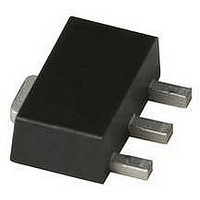
ATF-52189-BLK Avago Technologies US Inc., ATF-52189-BLK Datasheet - Page 2

ATF-52189-BLK
Manufacturer Part Number
ATF-52189-BLK
Description
IC PHEMT 2GHZ 4.5V 200MA SOT-89
Manufacturer
Avago Technologies US Inc.
Datasheet
1.ATF-52189-BLK.pdf
(18 pages)
Specifications of ATF-52189-BLK
Transistor Type
pHEMT FET
Frequency
2GHz
Gain
16dB
Voltage - Rated
7V
Current Rating
500mA
Noise Figure
1.5dB
Current - Test
200mA
Voltage - Test
4.5V
Power - Output
27dBm
Package / Case
SC-70-3, SOT-323-3
Drain Source Voltage Vds
7V
Continuous Drain Current Id
500mA
Power Dissipation Pd
1.5W
Noise Figure Typ
1.5dB
No. Of Pins
4
Peak Reflow Compatible (260 C)
Yes
No. Of Transistors
1
Current Gain-bandwidth Typ
6GHz
Marking, Smd
2Gx
Rohs Compliant
Yes
Current Gain-bandwidth Min
50MHz
Lead Free Status / RoHS Status
Lead free / RoHS Compliant
Available stocks
Company
Part Number
Manufacturer
Quantity
Price
Part Number:
ATF-52189-BLK
Manufacturer:
AVAGO/安华高
Quantity:
20 000
2
ATF-52189 Absolute Maximum Ratings
I
I
P
P
T
T
ATF-52189 Electrical Specifications
T
Symbol
Vgs
Vth
Ids
Gm
Igss
NF
G
OIP3
P1dB
PAE
NF
G
OIP3
P1dB
Symbol
V
V
V
ds
gs
ch
stg
diss
in max.
ds
gs
gd
A
= 25°C, DC bias for RF parameters is Vds = 4.5V and Ids = 200 mA unless otherwise specified.
Parameters and Test Conditions
Operational Gate Voltage
Threshold Voltage
Drain to Source Current
Transconductance
Gate Leakage Current
Noise Figure
Gain
Output 3
Output 1dB Compressed
Power Added Efficiency
Noise Figure
Gain
Output 3rd Order Intercept Point
Output 1dB Compressed
Parameter
Drain–Source Voltage
Gate–Source Voltage
Gate Drain Voltage
Drain Current
Gate Current
Total Power Dissipation
RF Input Power
Channel Temperature
Storage Temperature
[1]
[1]
rd
Order Intercept Point
[2]
[2]
[2]
[1]
[1]
[2]
[3]
[1]
[1]
[1]
Units
V
V
V
mA
mA
W
dBm
°C
°C
Vds = 4.5V, Ids = 200 mA
Vds = 4.5V, Ids = 16 mA
Vds = 4.5V, Vgs = 0V
Vds = 4.5V, Gm = ∆Ids/∆Vgs;
∆Vgs = Vgs1 – Vgs2
Vgs1 = 0.55V, Vgs2 = 0.5V
Vds = 0V, Vgs = -4V
f = 2 GHz
f = 900 MHz
f = 2 GHz
f = 900 MHz
f = 2 GHz
f = 900 MHz
f = 2 GHz
f = 900 MHz
f = 2 GHz
f = 900 MHz
f=900 MHz
f=2.0 GHz
f=2.4 GHz
f=900 MHz
f=2.0 GHz
f=2.4 GHz
f=900 MHz
f=2.0 GHz
f=2.4 GHz
f=900 MHz
f=2.0 GHz
f=2.4 GHz
Absolute
Maximum
7
-5 to 1.0
-5 to 1.0
500
46
1.5
+27
150
-65 to 150
Units
V
V
µA
mmho
µA
dB
dB
dB
dB
dBm
dBm
dBm
dBm
%
%
dB
dB
dB
dB
dB
dB
dBm
dBm
dBm
dBm
dBm
dBm
Notes:
1. Operation of this device above any one of
2. Assuming DC quiescent conditions.
3. Board (package belly) temperature T
4. Channel-to-board thermal resistance
these parameters may cause permanent
damage.
Derate 19.25 mW/°C for T
measured using 150°C Liquid Crystal
Measurement method.
Min.
—
—
—
—
-20.0
—
—
14.8
—
38.5
—
25.5
—
40.0
—
—
—
—
—
14.8
—
—
38.5
—
—
25.5
—
Thermal Resistance
θ
ch-b
continued on next page
= 52°C/W
Typ.
0.62
0.28
14.8
1300
0.49
1.50
1.25
16.0
16.5
42.0
42.0
27.0
27.2
55.0
50.0
1.25
1.50
1.60
16.5
16.0
13.5
42.0
42.0
41.0
27.2
27.0
26.0
B
> 72°C.
[2,4]
B
Max.
—
—
—
—
—
—
—
17.8
—
—
—
—
—
—
—
—
—
—
—
17.8
—
—
—
—
—
—
is 25°C.


