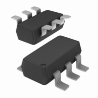
BC807DS,115 NXP Semiconductors, BC807DS,115 Datasheet - Page 2

BC807DS,115
Manufacturer Part Number
BC807DS,115
Description
TRANSISTOR PNP 500MA 45V SOT457
Manufacturer
NXP Semiconductors
Datasheet
1.BC807DS115.pdf
(7 pages)
Specifications of BC807DS,115
Package / Case
SC-74-6
Transistor Type
2 PNP (Dual)
Current - Collector (ic) (max)
500mA
Voltage - Collector Emitter Breakdown (max)
45V
Vce Saturation (max) @ Ib, Ic
700mV @ 50mA, 500mA
Dc Current Gain (hfe) (min) @ Ic, Vce
160 @ 100mA, 1V
Power - Max
370mW
Frequency - Transition
80MHz
Mounting Type
Surface Mount
Dc Collector/base Gain Hfe Min
40
Minimum Operating Temperature
- 65 C
Configuration
Dual
Transistor Polarity
PNP
Mounting Style
SMD/SMT
Collector- Emitter Voltage Vceo Max
- 45 V
Emitter- Base Voltage Vebo
- 5 V
Continuous Collector Current
- 500 mA
Maximum Dc Collector Current
- 1 A
Power Dissipation
370 mW
Maximum Operating Frequency
80 MHz
Maximum Operating Temperature
+ 150 C
Lead Free Status / RoHS Status
Lead free / RoHS Compliant
Current - Collector Cutoff (max)
-
Lead Free Status / Rohs Status
Lead free / RoHS Compliant
Other names
934057318115
BC807DS T/R
BC807DS T/R
BC807DS T/R
BC807DS T/R
NXP Semiconductors
FEATURES
• High current (500 mA)
• 600 mW total power dissipation
• Replaces two SOT23 packaged transistors on same
APPLICATIONS
• General purpose switching and amplification
• Push-pull amplifiers
• Multi-phase stepper motor drivers.
DESCRIPTION
PNP transistor pair in a SOT457 (SC-74) plastic package.
MARKING
LIMITING VALUES
In accordance with the Absolute Maximum Rating System (IEC 60134).
Note
1. Device mounted on a printed-circuit board; single sided copper; tinplated; mounting pad for collector 1 cm
2002 Nov 22
BC807DS
Per transistor unless otherwise specified
V
V
V
I
I
I
P
T
T
T
Per device
P
SYMBOL
C
CM
BM
PCB area.
stg
j
amb
CBO
CEO
EBO
tot
tot
PNP general purpose double transistor
TYPE NUMBER
collector-base voltage
collector-emitter voltage
emitter-base voltage
collector current (DC)
peak collector current
peak base current
total power dissipation
storage temperature
junction temperature
operating ambient temperature
total power dissipation
PARAMETER
MARKING CODE
N2
open emitter
open base
open collector
T
T
amb
amb
≤ 25 °C; note 1
≤ 25 °C; note 1
2
QUICK REFERENCE DATA
PINNING
V
I
I
SYMBOL
C
CM
CEO
Fig.1
CONDITIONS
PIN
1, 4
2, 5
6, 3
Top view
Simplified outline (SOT457) and symbol.
6
1
collector-emitter voltage
collector current (DC)
peak collector current
emitter
base
collector
5
2
PARAMETER
4
3
DESCRIPTION
MAM457
TR1; TR2
TR1; TR2
TR1; TR2
−
−
−
−
−
−
−
−65
−
−65
−
MIN.
TR1
Product data sheet
6
1
BC807DS
−45
−500
−1
−50
−45
−5
−500
−1
−200
370
+150
150
+150
600
MAX.
MAX.
5
2
2
4
3
TR2
.
V
mA
A
V
V
V
mA
A
mA
mW
°C
°C
°C
mW
UNIT
UNIT


