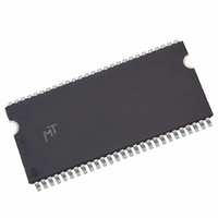
MT48LC4M16A2TG-7E IT:G Micron Technology Inc, MT48LC4M16A2TG-7E IT:G Datasheet - Page 47

MT48LC4M16A2TG-7E IT:G
Manufacturer Part Number
MT48LC4M16A2TG-7E IT:G
Description
DRAM Chip SDRAM 64M-Bit 4Mx16 3.3V 54-Pin TSOP-II Tray
Manufacturer
Micron Technology Inc
Type
SDRAMr
Datasheet
1.MT48LC4M16A2P-75G_TR.pdf
(72 pages)
Specifications of MT48LC4M16A2TG-7E IT:G
Density
64 Mb
Maximum Clock Rate
143 MHz
Package
54TSOP-II
Address Bus Width
14 Bit
Operating Supply Voltage
3.3 V
Maximum Random Access Time
5.4 ns
Operating Temperature
-40 to 85 °C
Format - Memory
RAM
Memory Type
SDRAM
Memory Size
64M (4M x 16)
Speed
143MHz
Interface
Parallel
Voltage - Supply
3 V ~ 3.6 V
Package / Case
54-TSOP II
Organization
4Mx16
Address Bus
14b
Access Time (max)
5.4ns
Operating Supply Voltage (typ)
3.3V
Package Type
TSOP-II
Operating Temp Range
-40C to 85C
Operating Supply Voltage (max)
3.6V
Operating Supply Voltage (min)
3V
Supply Current
150mA
Pin Count
54
Mounting
Surface Mount
Operating Temperature Classification
Industrial
Lead Free Status / RoHS Status
Contains lead / RoHS non-compliant
Table 14:
Table 15:
Table 16:
Table 17:
PDF: 09005aef80725c0b/Source: 09005aef806fc13c
64MSDRAM_2.fm - Rev. N 12/08 EN
Parameter/Condition
Parameter/Condition
Parameter
Parameter
Supply voltage
Input high voltage: Logic 1; All inputs
Input low voltage: Logic 0; All inputs
Input leakage current:
Any input 0V ≤ V
Output leakage current: DQs are disabled; 0V ≤ V
Output levels:
Output high voltage (Iout = –4mA)
Output low voltage (Iout = 4mA)
Operating current: active mode;
Burst = 2; READ or WRITE;
Standby current: Power-down mode;
All banks idle; CKE = LOW
Standby current: Active mode;
CKE = HIGH; CS# = HIGH; All banks active after
No accesses in progress
Operating current: Burst mode;
Page burst; READ or WRITE; All banks active
Auto refresh current:
CKE = HIGH; CS# = HIGH
Self refresh current:
CKE ≤ 0.2V
Input capacitance: CLK
Input capacitance: All other input-only pins
Input/output capacitance: DQs
Input capacitance: CLK
Input capacitance: All other input-only pins
Input/output capacitance: DQs
DC Electrical Characteristics and Operating Conditions
Notes 1, 5, 6 apply to entire table; notes appear on pages 50 and 51; V
I
Notes 1, 5, 6 apply to entire table; notes appear on pages 50 and 51; V
TSOP Capacitance
Note 2 applies to entire table; notes appear on pages 50 and 51
VFBGA Capacitance
Note 2 applies to entire table; notes appear on pages 50 and 51
DD
IN
Specifications and Conditions
≤ V
DD
(All other pins not under test = 0V)
t
RC ≥
t
RC (MIN)
t
t
t
Standard
Low power (L)
RFC =
RFC = 15.625µs
RFC = 3.906µs (AT)
t
RCD met;
OUT
t
RFC (MIN)
≤ V
DD
Q
47
V
Symbol
DD
Symbol
Symbol
Symbol
V
V
V
, V
I
I
I
I
I
I
I
I
I
V
OZ
DD
DD
DD
DD
DD
DD
DD
DD
OH
I
OL
IH
C
C
C
C
C
C
IL
I
Micron Technology, Inc., reserves the right to change products or specifications without notice.
DD
I
I
IO
I
I
IO
1
2
3
4
5
6
6
7
1
2
1
2
Q
150
180
250
0.5
60
-6
2
3
6
1
Min
Min
Min
–0.3
TBD
TBD
TBD
2.4
2.5
2.5
4.0
–5
–5
3
2
–
DD
DD
Max
125
150
230
, V
, V
-7E
0.5
64Mb: x4, x8, x16 SDRAM
45
2
3
6
1
Electrical Specifications
DD
V
DD
DD
Max
Max
Max
Q = +3.3V ±0.3V
Q = +3.3V ±0.3V
TBD
TBD
TBD
3.6
0.8
0.4
3.5
3.8
6.0
5
5
–
+ 0.3
©2000 Micron Technology, Inc. All rights reserved.
115
140
210
-75
0.5
45
2
3
6
1
Units
Units
Units
Units
µA
µA
pF
pF
pF
pF
pF
pF
mA
mA
mA
mA
mA
mA
V
V
V
V
V
19, 32, 33
3, 18, 19,
3, 12, 19,
3, 18, 19,
3, 12, 18,
Notes
Notes
Notes
Notes
22
22
32
32
32
32
29
30
31
29
30
31
4


