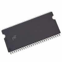
MT48LC4M16A2TG-7E IT:G Micron Technology Inc, MT48LC4M16A2TG-7E IT:G Datasheet - Page 61

MT48LC4M16A2TG-7E IT:G
Manufacturer Part Number
MT48LC4M16A2TG-7E IT:G
Description
DRAM Chip SDRAM 64M-Bit 4Mx16 3.3V 54-Pin TSOP-II Tray
Manufacturer
Micron Technology Inc
Type
SDRAMr
Datasheet
1.MT48LC4M16A2P-75G_TR.pdf
(72 pages)
Specifications of MT48LC4M16A2TG-7E IT:G
Density
64 Mb
Maximum Clock Rate
143 MHz
Package
54TSOP-II
Address Bus Width
14 Bit
Operating Supply Voltage
3.3 V
Maximum Random Access Time
5.4 ns
Operating Temperature
-40 to 85 °C
Format - Memory
RAM
Memory Type
SDRAM
Memory Size
64M (4M x 16)
Speed
143MHz
Interface
Parallel
Voltage - Supply
3 V ~ 3.6 V
Package / Case
54-TSOP II
Organization
4Mx16
Address Bus
14b
Access Time (max)
5.4ns
Operating Supply Voltage (typ)
3.3V
Package Type
TSOP-II
Operating Temp Range
-40C to 85C
Operating Supply Voltage (max)
3.6V
Operating Supply Voltage (min)
3V
Supply Current
150mA
Pin Count
54
Mounting
Surface Mount
Operating Temperature Classification
Industrial
Lead Free Status / RoHS Status
Contains lead / RoHS non-compliant
Figure 44:
PDF: 09005aef80725c0b/Source: 09005aef806fc13c
64MSDRAM_2.fm - Rev. N 12/08 EN
DQML, DQMH
A0–A9, A11
COMMAND
BA0, BA1
DQM /
CLK
A10
CKE
DQ
t CMS
t CKS
t AS
t AS
t AS
Alternating Bank Read Accesses
ACTIVE
BANK 0
T0
ROW
ROW
t CKH
t CMH
t AH
t AH
t AH
Notes:
t RCD - BANK 0
t RAS - BANK 0
t
t
RC - BANK 0
RRD
t CK
T1
1. For this example, BL = 4, and CL = 2.
2. x16: A8, A9 and A11 = “Don’t Care”
NOP
x8: A9 and A11 = “Don’t Care”
x4: A11 = “Don’t Care”
ENABLE AUTO PRECHARGE
t CMS
t CL
COLUMN m 2
BANK 0
T2
READ
t CMH
t CH
CAS Latency - BANK 0
T3
NOP
t LZ
t AC
61
BANK 3
ACTIVE
T4
ROW
ROW
D
OUT
t OH
t AC
m
t RCD - BANK 3
Micron Technology, Inc., reserves the right to change products or specifications without notice.
D
OUT
T5
NOP
m + 1
t OH
t AC
ENABLE AUTO PRECHARGE
COLUMN b 2
D
BANK 3
OUT
T6
READ
64Mb: x4, x8, x16 SDRAM
m + 2
t OH
t AC
CAS Latency - BANK 3
©2000 Micron Technology, Inc. All rights reserved.
t RP - BANK 0
D
T7
OUT
NOP
Timing Diagrams
m + 3
t OH
t AC
BANK 0
T8
ACTIVE
ROW
ROW
D
OUT
t RCD - BANK 0
t OH
DON’T CARE
UNDEFINED
t AC
b


