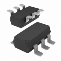
PBSS302PD,115 NXP Semiconductors, PBSS302PD,115 Datasheet - Page 3

PBSS302PD,115
Manufacturer Part Number
PBSS302PD,115
Description
TRANS PNP 40V 4A LOW SAT SOT457
Manufacturer
NXP Semiconductors
Datasheet
1.PBSS302PD115.pdf
(14 pages)
Specifications of PBSS302PD,115
Package / Case
SC-74-6
Transistor Type
PNP
Current - Collector (ic) (max)
4A
Voltage - Collector Emitter Breakdown (max)
40V
Vce Saturation (max) @ Ib, Ic
450mV @ 600mA, 6A
Current - Collector Cutoff (max)
100nA
Dc Current Gain (hfe) (min) @ Ic, Vce
175 @ 2A, 2V
Power - Max
1.1W
Frequency - Transition
110MHz
Mounting Type
Surface Mount
Dc Collector/base Gain Hfe Min
30
Minimum Operating Temperature
- 65 C
Configuration
Single Quad Collector
Transistor Polarity
PNP
Mounting Style
SMD/SMT
Collector- Emitter Voltage Vceo Max
40 V
Emitter- Base Voltage Vebo
5 V
Continuous Collector Current
- 4 A
Maximum Dc Collector Current
4 A
Power Dissipation
2500 mW
Maximum Operating Frequency
110 MHz (Typ)
Maximum Operating Temperature
+ 150 C
Lead Free Status / RoHS Status
Lead free / RoHS Compliant
Lead Free Status / RoHS Status
Lead free / RoHS Compliant, Lead free / RoHS Compliant
Other names
568-4152-2
934059132115
PBSS302PD T/R
PBSS302PD T/R
934059132115
PBSS302PD T/R
PBSS302PD T/R
NXP Semiconductors
PBSS302PD_2
Product data sheet
Table 5.
In accordance with the Absolute Maximum Rating System (IEC 60134).
[1]
[2]
[3]
[4]
[5]
Symbol
T
T
T
Fig 1. Power derating curves
j
amb
stg
Device mounted on a ceramic PCB, Al
Device mounted on an FR4 PCB, single-sided copper, tin-plated and standard footprint.
Device mounted on an FR4 PCB, single-sided copper, tin-plated, mounting pad for collector 1 cm
Device mounted on an FR4 PCB, single-sided copper, tin-plated, mounting pad for collector 6 cm
Operated under pulsed conditions: duty cycle
(1) Ceramic PCB, Al
(2) FR4 PCB, mounting pad for collector 6 cm
(3) FR4 PCB, mounting pad for collector 1 cm
(4) FR4 PCB, standard footprint
Limiting values
Parameter
junction temperature
ambient temperature
storage temperature
(mW)
Rev. 02 — 6 December 2007
P
1600
1200
2
tot
O
800
400
3
0
, standard footprint
…continued
75
25
2
(1)
(2)
(3)
(4)
O
Conditions
3
, standard footprint.
25
2
2
10 % and pulse width t
40 V, 4 A PNP low V
75
125
T
006aaa270
amb
( C)
Min
-
175
p
65
65
PBSS302PD
10 ms.
CEsat
© NXP B.V. 2007. All rights reserved.
Max
150
+150
+150
(BISS) transistor
Unit
C
C
C
2
2
.
.
3 of 14


