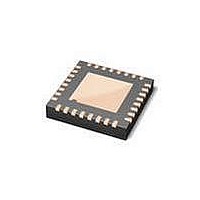
ISP1504CBS NXP Semiconductors, ISP1504CBS Datasheet - Page 14

ISP1504CBS
Manufacturer Part Number
ISP1504CBS
Description
RF Transceiver USB2.0 ULPI OTG TRANSCEIVER
Manufacturer
NXP Semiconductors
Datasheet
1.ISP1504ABS118.pdf
(83 pages)
Specifications of ISP1504CBS
Operating Supply Voltage
1.65 V to 3.6 V
Mounting Style
SMD/SMT
Package / Case
HVQFN
Minimum Operating Temperature
- 40 C
Lead Free Status / RoHS Status
Lead free / RoHS Compliant
Other names
ISP1504CBS,157
Available stocks
Company
Part Number
Manufacturer
Quantity
Price
Part Number:
ISP1504CBS
Manufacturer:
NXP/恩智浦
Quantity:
20 000
Company:
Part Number:
ISP1504CBSFA
Manufacturer:
NXP
Quantity:
6 041
NXP Semiconductors
ISP1504A_ISP1504C_3
Product data sheet
7.9.12 REG3V3 and REG1V8
7.9.13 XTAL1 and XTAL2
7.9.14 RESET_N
7.9.15 DIR
To prevent electrical overstress, it is strongly recommended that you attach a series
resistor on the V
internal charge pump. For details, see
Regulator output voltage. These supplies are used to power the ISP1504 internal digital
and analog circuits, and must not be used to power external circuits.
For correct operation of the regulator, it is recommended that you connect REG3V3 and
REG1V8 to decoupling capacitors. For examples, see
XTAL1 is the crystal input, and XTAL2 is the crystal output. The allowed frequency on the
XTAL1 pin depends on the ISP1504 product version.
If the link requires a 60 MHz clock from the ISP1504, then either a crystal must be
attached, or a clock of the same frequency must be driven into XTAL1, with XTAL2 left
floating.
If a crystal is attached, it requires external load capacitors to GND on each terminal of the
crystal. For details, see
If at any time the system wants to stop the clock on XTAL1, the link must first put the
ISP1504 into low-power mode. The clock on XTAL1 must be restarted before low-power
mode is exited.
An active LOW asynchronous reset pin that resets all circuits in the ISP1504. The
ISP1504 contains an internal power-on reset circuit, and therefore using the RESET_N
pin is optional. If RESET_N is not used, it must be connected to V
For details on using RESET_N, see
ULPI direction output pin. Controls the direction of the data bus. By default, the ISP1504
holds DIR at LOW, causing the data bus to be an input. When DIR is LOW, the ISP1504
listens for data from the link. The ISP1504 pulls DIR to HIGH only when it has data to
send to the link, which is for one of two reasons:
The DIR pin can also be 3-stated by driving CHIP_SELECT_N to HIGH.
For details on DIR usage, refer to UTMI+ Low Pin Interface (ULPI) Specification Rev. 1.1 .
•
•
To send the USB receive data, RXCMD status updates and register reads data to the
link.
To block the link from driving the data bus during power-up, reset and low-power
(suspend) mode.
BUS
pin (R
Section
Rev. 03 — 7 April 2008
VBUS
). R
16.
VBUS
Section
Section
must not be attached when using the ISP1504
9.3.2.
ISP1504A; ISP1504C
16.
Section
ULPI HS USB OTG transceiver
16.
CC(I/O)
© NXP B.V. 2008. All rights reserved.
.
13 of 82


