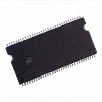
MT46V128M8P-6T:A Micron Technology Inc, MT46V128M8P-6T:A Datasheet - Page 76

MT46V128M8P-6T:A
Manufacturer Part Number
MT46V128M8P-6T:A
Description
DRAM Chip DDR SDRAM 1G-Bit 128Mx8 2.5V 66-Pin TSOP Tray
Manufacturer
Micron Technology Inc
Type
DDR SDRAMr
Datasheet
1.MT46V256M4P-6TA_TR.pdf
(82 pages)
Specifications of MT46V128M8P-6T:A
Density
1 Gb
Maximum Clock Rate
333 MHz
Package
66TSOP
Address Bus Width
16 Bit
Operating Supply Voltage
2.5 V
Maximum Random Access Time
0.7 ns
Operating Temperature
0 to 70 °C
Format - Memory
RAM
Memory Type
DDR SDRAM
Memory Size
1G (128M x 8)
Speed
6ns
Interface
Parallel
Voltage - Supply
2.3 V ~ 2.7 V
Package / Case
66-TSOP
Organization
128Mx8
Address Bus
16b
Access Time (max)
700ps
Operating Supply Voltage (typ)
2.5V
Package Type
TSOP
Operating Temp Range
0C to 70C
Operating Supply Voltage (max)
2.7V
Operating Supply Voltage (min)
2.3V
Supply Current
230mA
Pin Count
66
Mounting
Surface Mount
Operating Temperature Classification
Commercial
Lead Free Status / RoHS Status
Lead free / RoHS Compliant
Figure 48:
PRECHARGE
Auto Precharge
PDF: 09005aef80a2f898/Source: 09005aef82a95a3a
DDR_x4x8x16_Core2.fm - 1Gb DDR: Rev. I, Core DDR: Rev. B 12/07 EN
Data Input Timing
Notes:
1. WRITE command issued at T0.
2.
3.
4. For x16, LDQS controls the lower byte and UDQS controls the upper byte.
5. DI b = data-in from column b.
The bank(s) will be available for a subsequent row access a specified time (
PRECHARGE command is issued, except in the case of concurrent auto precharge. With
concurrent auto precharge, a READ or WRITE command to a different bank is allowed as
long as it does not interrupt the data transfer in the current bank and does not violate
any other timing parameters. Input A10 determines whether one or all banks are to be
precharged, and in the case where only one bank is to be precharged, inputs BA0, BA1
select the bank. When all banks are to be precharged, BA0, BA1 are treated as “Don’t
Care.” Once a bank has been precharged, it is in the idle state and must be activated
prior to any READ or WRITE commands being issued to that bank. A PRECHARGE
command will be treated as a NOP if there is no open row in that bank (idle state), or if
the previously open row is already in the process of precharging.
Auto precharge is a feature which performs the same individual-bank precharge func-
tion described above, but without requiring an explicit command. This is accomplished
by using A10 to enable auto precharge in conjunction with a specific READ or WRITE
command. A precharge of the bank/row that is addressed with the READ or WRITE
command is automatically performed upon completion of the READ or WRITE burst.
Auto precharge is either enabled or disabled for each individual READ or WRITE
command. This device supports concurrent auto precharge if the command to the other
bank does not interrupt the data transfer to the current bank.
Auto precharge ensures that the precharge is initiated at the earliest valid stage within a
burst. This “earliest valid stage” is determined as if an explicit PRECHARGE command
was issued at the earliest possible time, without violating
each burst type in “Operations” on page 43. The user must not issue another command
to the same bank until the precharge time (
DQS
CK#
DM
DQ
CK
t
t
DSH (MIN) generally occurs during
DSS (MIN) generally occurs during
T0
1
t DQSS
t WPRES
t DS
t WPRE
DI
T1
b
t DSH 2
t DH
76
T1n
t DQSL
t DSS 3
t
t
Transitioning Data
DQSS (MAX).
DQSS (MIN).
T2
Micron Technology, Inc., reserves the right to change products or specifications without notice.
t DQSH
t DSH 2
t
RP) is completed.
T2n
t WPST
t DSS 3
1Gb: x4, x8, x16 DDR SDRAM
T3
Don’t Care
t
RAS (MIN), as described for
©2003 Micron Technology, Inc. All rights reserved.
Operations
t
RP) after the


