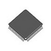
82P2282PF IDT, Integrated Device Technology Inc, 82P2282PF Datasheet - Page 15

82P2282PF
Manufacturer Part Number
82P2282PF
Description
Manufacturer
IDT, Integrated Device Technology Inc
Datasheet
1.82P2282PF.pdf
(381 pages)
Specifications of 82P2282PF
Screening Level
Industrial
Pin Count
100
Mounting
Surface Mount
Package Type
TQFP
Operating Temperature (min)
-40C
Operating Temperature (max)
85C
Lead Free Status / RoHS Status
Not Compliant
- Current page: 15 of 381
- Download datasheet (3Mb)
IDT82P2282
2
Note:
* The contents in the brackets indicate the position of the preceding bit and the address of the register. After the address, if the punctuation ‘,...’ is followed, this bit is in a per-link control reg-
ister and the listed address belongs to Link 1. Users can find the omitted addresses in Chapter 5. If there is no punctuation followed the address, this bit is in a global control register.
Pin Description
RSIG[1] / MRSIG
RSD[1] / MRSD
RRING[1]
RRING[2]
TRING[1]
TRING[2]
RSIG[2]
RTIP[1]
RTIP[2]
TTIP[1]
TTIP[2]
RSD[2]
Name
PIN DESCRIPTION
Output
Output
Output
Type
Input
Pin No.
27
12
28
11
21
18
22
17
79
71
78
70
RTIP[1:2] / RRING[1:2]: Receive Bipolar Tip/Ring for Link 1 ~ 2
These pins are the differential line receiver inputs.
TTIP[1:2] / TRING[1:2]: Transmit Bipolar Tip/Ring for Link 1 ~ 2
These pins are the differential line driver outputs and can be set to high impedance state globally or individually. A logic
high on the THZ pin sets all these pins to high impedance state. When the T_HZ bit (b4, T1/J1-023H,... / b4, E1-
023H,...) * is set to ‘1’, the TTIPn/TRINGn pins in the corresponding link are set to high impedance state.
Besides, TTIPn/TRINGn will also be set to high impedance state by other ways (refer to Chapter 3.25 Line Driver for
details).
RSD[1:2]: Receive Side System Data for Link 1 ~ 2
The processed data stream is output on these pins.
In Receive Clock Master mode, the RSDn pins are updated on the active edge of the corresponding RSCKn.
In Receive Clock Slave mode, selected by the RSLVCK bit (b4, T1/J1-010H / b4, E1-010H), the RSDn pins are
updated on the active edge of the corresponding RSCKn or both two RSDn pins are updated on the active edge of
RSCK[1].
MRSD: Multiplexed Receive Side System Data for Link 1 ~ 2
In Receive Multiplexed mode, the MRSD pin is used to output the processed data stream. Using a byte-interleaved
multiplexing scheme, the MRSD pin outputs the data from Link 1 and Link 2. The data on the MRSD pin is updated on
the active edge of the MRSCK.
RSIG[1:2]: Receive Side System Signaling for Link 1 ~ 2
The extracted signaling bits are output on these pins. They are located in the lower nibble (b5 ~ b8) and are channel/
timeslot-aligned with the data output on the corresponding RSDn pin.
In Receive Clock Master mode, the RSIGn pins are updated on the active edge of the corresponding RSCKn.
In Receive Clock Slave mode, selected by the RSLVCK bit (b4, T1/J1-010H / b4, E1-010H), the RSIGn pins are
updated on the active edge of the corresponding RSCKn or both two RSIGn are updated on the active edge of
RSCK[1].
MRSIG: Multiplexed Receive Side System Signaling for Link 1 ~ 2
In Receive Multiplexed mode, the MRSIG pin is used to output the extracted signaling bits. The signaling bits are
located in the lower nibble (b5 ~ b8) and are channel/timeslot-aligned with the data output on the MRSD pin. Using the
byte-interleaved multiplexing scheme, the MRSIG pin outputs the signaling bits from Link 1 and Link 2. The signaling
bits on the MRSIG pin is updated on the active edge of the MRSCK.
Line and System Interface
15
DUAL T1/E1/J1 LONG HAUL / SHORT HAUL TRANSCEIVER
Description
August 20, 2009
Related parts for 82P2282PF
Image
Part Number
Description
Manufacturer
Datasheet
Request
R

Part Number:
Description:
TRANSLATION DEVICE DPI 80-PQFP
Manufacturer:
IDT, Integrated Device Technology Inc
Datasheet:

Part Number:
Description:
IDT PART
Manufacturer:
IDT, Integrated Device Technology Inc
Datasheet:

Part Number:
Description:
IC LIU T1/E1/J1 OCTAL 256PBGA
Manufacturer:
IDT, Integrated Device Technology Inc
Datasheet:

Part Number:
Description:
IC FREQ TIMING GENERATOR 28TSSOP
Manufacturer:
IDT, Integrated Device Technology Inc
Datasheet:

Part Number:
Description:
IC CLK DVR PLL 1:10 40VFQFPN
Manufacturer:
IDT, Integrated Device Technology Inc
Datasheet:

Part Number:
Description:
IC CLK FANOUT BUFFER 1:18 32LQFP
Manufacturer:
IDT, Integrated Device Technology Inc
Datasheet:

Part Number:
Description:
IC CLK FANOUT BUFFER 1:18 32LQFP
Manufacturer:
IDT, Integrated Device Technology Inc
Datasheet:

Part Number:
Description:
IC CK505 VREG/RES 56TSSOP
Manufacturer:
IDT, Integrated Device Technology Inc
Datasheet:

Part Number:
Description:
IC SDRAM CLK DVR 1:10 48-TSSOP
Manufacturer:
IDT, Integrated Device Technology Inc
Datasheet:

Part Number:
Description:
IC CLK DVR PLL 1:10 48TSSOP
Manufacturer:
IDT, Integrated Device Technology Inc
Datasheet:

Part Number:
Description:
IC FLEXPC CLK PROGR P4 56-TSSOP
Manufacturer:
IDT, Integrated Device Technology Inc
Datasheet:

Part Number:
Description:
IC FLEXPC CLK PROGR P4 56-TSSOP
Manufacturer:
IDT, Integrated Device Technology Inc
Datasheet:

Part Number:
Description:
IC FLEXPC CLK PROGR P4 56-SSOP
Manufacturer:
IDT, Integrated Device Technology Inc
Datasheet:

Part Number:
Description:
IC PLL CLK DRIVER 2.5V 28-TSSOP
Manufacturer:
IDT, Integrated Device Technology Inc
Datasheet:

Part Number:
Description:
IC CLOCK DRIVER 2.5V 24-TSSOP
Manufacturer:
IDT, Integrated Device Technology Inc
Datasheet:


