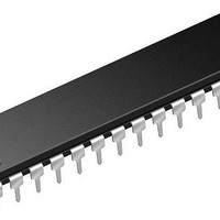
PIC16F1518-E/SP Microchip Technology, PIC16F1518-E/SP Datasheet - Page 224

PIC16F1518-E/SP
Manufacturer Part Number
PIC16F1518-E/SP
Description
28-pin, 28KB Flash, 1024B RAM, 10-bit ADC, 2xCCP, SPI, MI2C, EUSART, 2.3V-5.5V 2
Manufacturer
Microchip Technology
Series
PIC® XLP™ 16Fr
Datasheet
1.PIC16F1516-EMV.pdf
(344 pages)
Specifications of PIC16F1518-E/SP
Processor Series
PIC16F151x
Core
PIC
Data Bus Width
8 bit
Program Memory Type
Flash
Program Memory Size
16 KB
Data Ram Size
1 KB
Interface Type
I2C, SPI, USART
Maximum Clock Frequency
20 MHz
Number Of Programmable I/os
25
Number Of Timers
3
Operating Supply Voltage
2.3 V to 5.5 V
Maximum Operating Temperature
+ 125 C
Mounting Style
Through Hole
Package / Case
PDIP-28
Core Processor
PIC
Core Size
8-Bit
Speed
20MHz
Connectivity
I²C, LIN, SPI, UART/USART
Peripherals
Brown-out Detect/Reset, POR, PWM, WDT
Number Of I /o
25
Eeprom Size
-
Ram Size
1K x 8
Voltage - Supply (vcc/vdd)
2.3 V ~ 5.5 V
Data Converters
A/D 17x10b
Oscillator Type
Internal
Operating Temperature
-40°C ~ 125°C
Lead Free Status / Rohs Status
Details
- Current page: 224 of 344
- Download datasheet (3Mb)
PIC16(L)F1516/7/8/9
21.6.8
An Acknowledge sequence is enabled by setting the
Acknowledge Sequence Enable bit, ACKEN bit of the
SSPCON2 register. When this bit is set, the SCL pin is
pulled low and the contents of the Acknowledge data bit
are presented on the SDA pin. If the user wishes to gen-
erate an Acknowledge, then the ACKDT bit should be
cleared. If not, the user should set the ACKDT bit before
starting an Acknowledge sequence. The Baud Rate
Generator then counts for one rollover period (T
and the SCL pin is deasserted (pulled high). When the
SCL pin is sampled high (clock arbitration), the Baud
Rate Generator counts for T
pulled low. Following this, the ACKEN bit is automatically
cleared, the Baud Rate Generator is turned off and the
MSSP module then goes into Idle mode
21.6.8.1
If the user writes the SSPBUF when an Acknowledge
sequence is in progress, then WCOL is set and the
contents of the buffer are unchanged (the write does
not occur).
FIGURE 21-30:
FIGURE 21-31:
DS41452B-page 224
Note: T
Note: T
ACKNOWLEDGE SEQUENCE
TIMING
SCL
SDA
WCOL Status Flag
SSPIF
Write to SSPCON2,
Falling edge of
9th clock
BRG
BRG
SDA
SCL
Acknowledge sequence starts here,
= one Baud Rate Generator period.
= one Baud Rate Generator period.
ACKNOWLEDGE SEQUENCE WAVEFORM
STOP CONDITION RECEIVE OR TRANSMIT MODE
ACK
set PEN
SSPIF set at
the end of receive
BRG
ACKEN = 1, ACKDT = 0
. The SCL pin is then
write to SSPCON2
T
T
(Figure
BRG
BRG
SDA asserted low before rising edge of clock
to setup Stop condition
8
D0
21-29).
T
SCL brought high after T
BRG
BRG
Preliminary
)
Cleared in
software
P
T
SCL = 1 for T
after SDA sampled high. P bit (SSPSTAT<4>) is set.
BRG
T
BRG
ACK
21.6.9
A Stop bit is asserted on the SDA pin at the end of a
receive/transmit by setting the Stop Sequence Enable
bit, PEN bit of the SSPCON2 register. At the end of a
receive/transmit, the SCL line is held low after the
falling edge of the ninth clock. When the PEN bit is set,
the master will assert the SDA line low. When the SDA
line is sampled low, the Baud Rate Generator is
reloaded and counts down to ‘0’. When the Baud Rate
Generator times out, the SCL pin will be brought high
and one T
later, the SDA pin will be deasserted. When the SDA
pin is sampled high while SCL is high, the P bit of the
SSPSTAT register is set. A T
cleared and the SSPIF bit is set
21.6.9.1
If the user writes the SSPBUF when a Stop sequence
is in progress, then the WCOL bit is set and the
contents of the buffer are unchanged (the write does
not occur).
PEN bit (SSPCON2<2>) is cleared by
T
hardware and the SSPIF bit is set
BRG
9
BRG
BRG
SSPIF set at the end
of Acknowledge sequence
, followed by SDA = 1 for T
BRG
STOP CONDITION TIMING
WCOL Status Flag
ACKEN automatically cleared
(Baud Rate Generator rollover count)
2011 Microchip Technology Inc.
Cleared in
software
BRG
BRG
(Figure
later, the PEN bit is
21-30).
Related parts for PIC16F1518-E/SP
Image
Part Number
Description
Manufacturer
Datasheet
Request
R

Part Number:
Description:
IC, 8BIT MCU, PIC16F, 32MHZ, SOIC-18
Manufacturer:
Microchip Technology
Datasheet:

Part Number:
Description:
IC, 8BIT MCU, PIC16F, 32MHZ, SSOP-20
Manufacturer:
Microchip Technology
Datasheet:

Part Number:
Description:
IC, 8BIT MCU, PIC16F, 32MHZ, DIP-18
Manufacturer:
Microchip Technology
Datasheet:

Part Number:
Description:
IC, 8BIT MCU, PIC16F, 32MHZ, QFN-28
Manufacturer:
Microchip Technology
Datasheet:

Part Number:
Description:
IC, 8BIT MCU, PIC16F, 32MHZ, QFN-28
Manufacturer:
Microchip Technology
Datasheet:

Part Number:
Description:
IC, 8BIT MCU, PIC16F, 32MHZ, QFN-28
Manufacturer:
Microchip Technology
Datasheet:

Part Number:
Description:
IC, 8BIT MCU, PIC16F, 32MHZ, SSOP-20
Manufacturer:
Microchip Technology
Datasheet:

Part Number:
Description:
IC, 8BIT MCU, PIC16F, 20MHZ, DIP-40
Manufacturer:
Microchip Technology
Datasheet:

Part Number:
Description:
IC, 8BIT MCU, PIC16F, 32MHZ, QFN-28
Manufacturer:
Microchip Technology
Datasheet:

Part Number:
Description:
IC, 8BIT MCU, PIC16F, 20MHZ, MQFP-44
Manufacturer:
Microchip Technology
Datasheet:

Part Number:
Description:
IC, 8BIT MCU, PIC16F, 20MHZ, QFN-20
Manufacturer:
Microchip Technology
Datasheet:

Part Number:
Description:
IC, 8BIT MCU, PIC16F, 32MHZ, QFN-28
Manufacturer:
Microchip Technology
Datasheet:

Part Number:
Description:
MCU 14KB FLASH 768B RAM 64-TQFP
Manufacturer:
Microchip Technology
Datasheet:

Part Number:
Description:
7 KB Flash, 384 Bytes RAM, 32 MHz Int. Osc, 16 I/0, Enhanced Mid Range Core, Low
Manufacturer:
Microchip Technology

Part Number:
Description:
14KB Flash, 512B RAM, 256B EEPROM, LCD, 1.8-5.5V 40 UQFN 5x5x0.5mm TUBE
Manufacturer:
Microchip Technology
Datasheet:


