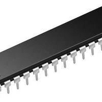
PIC16F1518-E/SP Microchip Technology, PIC16F1518-E/SP Datasheet - Page 264

PIC16F1518-E/SP
Manufacturer Part Number
PIC16F1518-E/SP
Description
28-pin, 28KB Flash, 1024B RAM, 10-bit ADC, 2xCCP, SPI, MI2C, EUSART, 2.3V-5.5V 2
Manufacturer
Microchip Technology
Series
PIC® XLP™ 16Fr
Datasheet
1.PIC16F1516-EMV.pdf
(344 pages)
Specifications of PIC16F1518-E/SP
Processor Series
PIC16F151x
Core
PIC
Data Bus Width
8 bit
Program Memory Type
Flash
Program Memory Size
16 KB
Data Ram Size
1 KB
Interface Type
I2C, SPI, USART
Maximum Clock Frequency
20 MHz
Number Of Programmable I/os
25
Number Of Timers
3
Operating Supply Voltage
2.3 V to 5.5 V
Maximum Operating Temperature
+ 125 C
Mounting Style
Through Hole
Package / Case
PDIP-28
Core Processor
PIC
Core Size
8-Bit
Speed
20MHz
Connectivity
I²C, LIN, SPI, UART/USART
Peripherals
Brown-out Detect/Reset, POR, PWM, WDT
Number Of I /o
25
Eeprom Size
-
Ram Size
1K x 8
Voltage - Supply (vcc/vdd)
2.3 V ~ 5.5 V
Data Converters
A/D 17x10b
Oscillator Type
Internal
Operating Temperature
-40°C ~ 125°C
Lead Free Status / Rohs Status
Details
- Current page: 264 of 344
- Download datasheet (3Mb)
PIC16(L)F1516/7/8/9
22.6
The EUSART will remain active during Sleep only in the
Synchronous Slave mode. All other modes require the
system clock and therefore cannot generate the neces-
sary signals to run the Transmit or Receive Shift regis-
ters during Sleep.
Synchronous Slave mode uses an externally generated
clock to run the Transmit and Receive Shift registers.
22.6.1
To receive during Sleep, all the following conditions
must be met before entering Sleep mode:
• RCSTA and TXSTA Control registers must be
• If interrupts are desired, set the RCIE bit of the
• The RCIF interrupt flag must be cleared by read-
Upon entering Sleep mode, the device will be ready to
accept data and clocks on the RX/DT and TX/CK pins,
respectively. When the data word has been completely
clocked in by the external device, the RCIF interrupt
flag bit of the PIR1 register will be set. Thereby, waking
the processor from Sleep.
Upon waking from Sleep, the instruction following the
SLEEP instruction will be executed. If the Global Inter-
rupt Enable (GIE) bit of the INTCON register is also set,
then the Interrupt Service Routine at address 004h will
be called.
DS41452B-page 264
configured for Synchronous Slave Reception (see
Section 22.5.2.4 “Synchronous Slave
Reception Set-up:”
PIE1 register and the GIE and PEIE bits of the
INTCON register.
ing RCREG to unload any pending characters in
the receive buffer.
EUSART Operation During Sleep
SYNCHRONOUS RECEIVE DURING
SLEEP
).
Preliminary
22.6.2
To transmit during Sleep, all the following conditions
must be met before entering Sleep mode:
• RCSTA and TXSTA Control registers must be
• The TXIF interrupt flag must be cleared by writing
• If interrupts are desired, set the TXIE bit of the
• Interrupt enable bits TXIE of the PIE1 register and
Upon entering Sleep mode, the device will be ready to
accept clocks on TX/CK pin and transmit data on the
RX/DT pin. When the data word in the TSR has been
completely clocked out by the external device, the
pending byte in the TXREG will transfer to the TSR and
the TXIF flag will be set. Thereby, waking the processor
from Sleep. At this point, the TXREG is available to
accept another character for transmission, which will
clear the TXIF flag.
Upon waking from Sleep, the instruction following the
SLEEP instruction will be executed. If the Global
Interrupt Enable (GIE) bit is also set then the Interrupt
Service Routine at address 0004h will be called.
configured for Synchronous Slave Transmission
(see
Transmission Set-up:”
the output data to the TXREG, thereby filling the
TSR and transmit buffer.
PIE1 register and the PEIE bit of the INTCON reg-
ister.
PEIE of the INTCON register must set.
Section 22.5.2.2 “Synchronous Slave
SYNCHRONOUS TRANSMIT
DURING SLEEP
2011 Microchip Technology Inc.
).
Related parts for PIC16F1518-E/SP
Image
Part Number
Description
Manufacturer
Datasheet
Request
R

Part Number:
Description:
IC, 8BIT MCU, PIC16F, 32MHZ, SOIC-18
Manufacturer:
Microchip Technology
Datasheet:

Part Number:
Description:
IC, 8BIT MCU, PIC16F, 32MHZ, SSOP-20
Manufacturer:
Microchip Technology
Datasheet:

Part Number:
Description:
IC, 8BIT MCU, PIC16F, 32MHZ, DIP-18
Manufacturer:
Microchip Technology
Datasheet:

Part Number:
Description:
IC, 8BIT MCU, PIC16F, 32MHZ, QFN-28
Manufacturer:
Microchip Technology
Datasheet:

Part Number:
Description:
IC, 8BIT MCU, PIC16F, 32MHZ, QFN-28
Manufacturer:
Microchip Technology
Datasheet:

Part Number:
Description:
IC, 8BIT MCU, PIC16F, 32MHZ, QFN-28
Manufacturer:
Microchip Technology
Datasheet:

Part Number:
Description:
IC, 8BIT MCU, PIC16F, 32MHZ, SSOP-20
Manufacturer:
Microchip Technology
Datasheet:

Part Number:
Description:
IC, 8BIT MCU, PIC16F, 20MHZ, DIP-40
Manufacturer:
Microchip Technology
Datasheet:

Part Number:
Description:
IC, 8BIT MCU, PIC16F, 32MHZ, QFN-28
Manufacturer:
Microchip Technology
Datasheet:

Part Number:
Description:
IC, 8BIT MCU, PIC16F, 20MHZ, MQFP-44
Manufacturer:
Microchip Technology
Datasheet:

Part Number:
Description:
IC, 8BIT MCU, PIC16F, 20MHZ, QFN-20
Manufacturer:
Microchip Technology
Datasheet:

Part Number:
Description:
IC, 8BIT MCU, PIC16F, 32MHZ, QFN-28
Manufacturer:
Microchip Technology
Datasheet:

Part Number:
Description:
MCU 14KB FLASH 768B RAM 64-TQFP
Manufacturer:
Microchip Technology
Datasheet:

Part Number:
Description:
7 KB Flash, 384 Bytes RAM, 32 MHz Int. Osc, 16 I/0, Enhanced Mid Range Core, Low
Manufacturer:
Microchip Technology

Part Number:
Description:
14KB Flash, 512B RAM, 256B EEPROM, LCD, 1.8-5.5V 40 UQFN 5x5x0.5mm TUBE
Manufacturer:
Microchip Technology
Datasheet:


