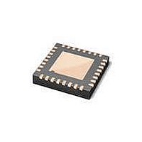
ISP1504ABS,118 NXP Semiconductors, ISP1504ABS,118 Datasheet - Page 26

ISP1504ABS,118
Manufacturer Part Number
ISP1504ABS,118
Description
RF Transceiver USB ULPI TRANSCEIVER
Manufacturer
NXP Semiconductors
Datasheet
1.ISP1504ABS118.pdf
(83 pages)
Specifications of ISP1504ABS,118
Number Of Transceivers
1
Esd Protection
YeskV
Operating Supply Voltage (typ)
Not RequiredV
Operating Temperature Classification
Industrial
Operating Supply Voltage (max)
Not RequiredV
Operating Supply Voltage (min)
Not RequiredV
Pin Count
32
Mounting
Surface Mount
Operating Temperature (max)
85C
Operating Temperature (min)
-40C
Operating Supply Voltage
1.65 V to 3.6 V
Mounting Style
SMD/SMT
Package / Case
HVQFN-32
Lead Free Status / RoHS Status
Compliant
Other names
935278308118 ISP1504ABS-T
NXP Semiconductors
ISP1504A_ISP1504C_3
Product data sheet
9.4.1 Driving 5 V on V
9.4.2 Fault detection
9.5.1 TXCMD
9.4 V
9.5 TXCMD and RXCMD
The ISP1504 provides a built-in charge pump. To enable the charge pump, the link must
set the DRV_VBUS bit in the OTG Control register.
The ISP1504 also supports external 5 V supplies. The ISP1504 can control the external
supply using the active-LOW PSW_N open-drain output pin. To enable the external supply
by driving PSW_N to LOW, the link must set the DRV_VBUS_EXT bit in the OTG Control
register to logic 1. The link can optionally set both the DRV_VBUS and DRV_VBUS_EXT
bits to logic 1 to enable the external supply.
Table 9
Table 9.
The ISP1504 supports external V
indicator signal. The indicator signal must be connected to the FAULT pin. To enable the
ISP1504 to monitor the digital fault input, the link must set the USE_EXT_VBUS_IND bit
in the OTG Control register and the IND_PASSTHRU bit in the Interface Control register to
logic 1. For details, see
The FAULT input pin is mapped to the A_VBUS_VLD bit in RXCMD. Any changes for the
FAULT input will trigger RXCMD carrying the FAULT condition with A_VBUS_VLD.
Commands between the ISP1504 and the link are described in the following subsections.
By default, the link must drive the ULPI bus to its idle state of 00h. To send commands and
USB packets, the link drives a nonzero value on DATA[7:0] to the ISP1504 by sending a
byte called TXCMD. Commands include USB packet transmissions, and register reads
and writes. Once the TXCMD is interpreted and accepted by the ISP1504, the NXT signal
is asserted and the link can follow up with the required number of data bytes. The TXCMD
byte format is given in
may result in undefined behavior.
Various TXCMD packet and register sequences are shown in later sections.
DRV_VBUS
0
1
X
BUS
power and fault detection
summarizes settings to drive 5 V on V
OTG Control register power control bits
DRV_VBUS_EXT
0
0
1
BUS
Table
Figure
Rev. 03 — 7 April 2008
10. Any values other than those in
11.
BUS
Power source used
internal and external V
internal V
external 5 V V
fault detector circuits that output a digital fault
BUS
ISP1504A; ISP1504C
BUS
charge pump is enabled
BUS
.
supply is enabled
BUS
ULPI HS USB OTG transceiver
power sources are disabled
Table 10
© NXP B.V. 2008. All rights reserved.
are illegal and
25 of 82


