TDA8351N6 NXP Semiconductors, TDA8351N6 Datasheet - Page 4
TDA8351N6
Manufacturer Part Number
TDA8351N6
Description
Manufacturer
NXP Semiconductors
Datasheet
1.TDA8351N6.pdf
(16 pages)
Specifications of TDA8351N6
Lead Free Status / RoHS Status
Compliant
Available stocks
Company
Part Number
Manufacturer
Quantity
Price


Philips Semiconductors
PINNING
1999 Sep 27
I
I
V
V
GND
V
V
V
V
drive(pos)
drive(neg)
P
O(B)
FB
O(A)
O(guard)
I(fb)
DC-coupled vertical deflection circuit
SYMBOL
Metal block connected to substrate pin 5.
Metal on back.
handbook, 2 columns
I drive(neg)
I drive(pos)
V O(guard)
V O(B)
V O(A)
V I(fb)
GND
V FB
V P
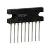
Fig.2 Pin configuration.
PIN
1
2
3
4
5
6
7
8
9
3
4
1
2
5
6
7
8
9
input power-stage (positive);
includes I
input power-stage (negative);
includes I
operating supply voltage
output voltage B
ground
input flyback supply voltage
output voltage A
guard output voltage
input feedback voltage
TDA8351
MBC989
DESCRIPTION
I(sb)
I(sb)
signal bias
signal bias
4
FUNCTIONAL DESCRIPTION
The vertical driver circuit is a bridge configuration. The
deflection coil is connected between the output amplifiers,
which are driven in opposite phase. An external resistor
(R
internal feedback information. The differential input circuit
is voltage driven. The input circuit has been adapted to
enable it to be used with the TDA9150, TDA9151B,
TDA9160A, TDA9162, TDA8366 and TDA8376 which
deliver symmetrical current signals. An external resistor
(R
determines the output current through the deflection coil.
The relationship between the differential input current and
the output current is defined by: I
The output current is adjustable from 0.5 A (p-p) to 3 A
(p-p) by varying R
voltage is 1.8 V. In the application it is recommended that
V
spread of input current and the spread in the value of
R
The flyback voltage is determined by an additional supply
voltage V
voltages (class G) makes it possible to fix the supply
voltage V
supply voltage V
this method, very high efficiency is achieved.
The supply voltage V
flyback voltage across the coil, this being possible due to
the absence of a decoupling capacitor (not necessary,
due to the bridge configuration). Built-in protections are:
A guard circuit V
activated at the following conditions:
This signal can be used for blanking the picture tube
screen.
diff
CON
during flyback
during short-circuit of the coil and during short-circuit of
the output pins (pins 4 and 7) to V
during open loop
when the thermal protection is activated.
M
CON
thermal protection
short-circuit protection of the output pins (pins 4 and 7)
short-circuit protection of the output pins to V
) connected in series with the deflection coil provides
= 1.5 V (typ). This is recommended because of the
.
) connected between the differential input
FB
P
optimum for the scan voltage and the second
. The principle of operating with two supply
FB
O(guard)
M
optimum for the flyback voltage. Using
. The maximum input differential
FB
is almost totally available as
is provided. The guard circuit is
diff
Product specification
P
R
or ground
CON
TDA8351
= I
coil
P
.
R
M
.
Related parts for TDA8351N6
Image
Part Number
Description
Manufacturer
Datasheet
Request
R

Part Number:
Description:
Tuners Gain-cntrlled IF Amp 5V
Manufacturer:
Infineon Technologies
Datasheet:

Part Number:
Description:
NXP Semiconductors designed the LPC2420/2460 microcontroller around a 16-bit/32-bitARM7TDMI-S CPU core with real-time debug interfaces that include both JTAG andembedded trace
Manufacturer:
NXP Semiconductors
Datasheet:

Part Number:
Description:
NXP Semiconductors designed the LPC2458 microcontroller around a 16-bit/32-bitARM7TDMI-S CPU core with real-time debug interfaces that include both JTAG andembedded trace
Manufacturer:
NXP Semiconductors
Datasheet:
Part Number:
Description:
NXP Semiconductors designed the LPC2468 microcontroller around a 16-bit/32-bitARM7TDMI-S CPU core with real-time debug interfaces that include both JTAG andembedded trace
Manufacturer:
NXP Semiconductors
Datasheet:
Part Number:
Description:
NXP Semiconductors designed the LPC2470 microcontroller, powered by theARM7TDMI-S core, to be a highly integrated microcontroller for a wide range ofapplications that require advanced communications and high quality graphic displays
Manufacturer:
NXP Semiconductors
Datasheet:
Part Number:
Description:
NXP Semiconductors designed the LPC2478 microcontroller, powered by theARM7TDMI-S core, to be a highly integrated microcontroller for a wide range ofapplications that require advanced communications and high quality graphic displays
Manufacturer:
NXP Semiconductors
Datasheet:
Part Number:
Description:
The Philips Semiconductors XA (eXtended Architecture) family of 16-bit single-chip microcontrollers is powerful enough to easily handle the requirements of high performance embedded applications, yet inexpensive enough to compete in the market for hi
Manufacturer:
NXP Semiconductors
Datasheet:
Part Number:
Description:
The XA-S3 device is a member of Philips Semiconductors? XA(eXtended Architecture) family of high performance 16-bitsingle-chip microcontrollers
Manufacturer:
NXP Semiconductors
Datasheet:

Part Number:
Description:
The NXP BlueStreak LH75401/LH75411 family consists of two low-cost 16/32-bit System-on-Chip (SoC) devices
Manufacturer:
NXP Semiconductors
Datasheet:
Part Number:
Description:
The NXP LPC3130/3131 combine an 180 MHz ARM926EJ-S CPU core, high-speed USB2
Manufacturer:
NXP Semiconductors
Datasheet:
Part Number:
Description:
The NXP LPC3141 combine a 270 MHz ARM926EJ-S CPU core, High-speed USB 2
Manufacturer:
NXP Semiconductors
Part Number:
Description:
The NXP LPC3143 combine a 270 MHz ARM926EJ-S CPU core, High-speed USB 2
Manufacturer:
NXP Semiconductors

Part Number:
Description:
The NXP LPC3152 combines an 180 MHz ARM926EJ-S CPU core, High-speed USB 2
Manufacturer:
NXP Semiconductors
Part Number:
Description:
The NXP LPC3154 combines an 180 MHz ARM926EJ-S CPU core, High-speed USB 2
Manufacturer:
NXP Semiconductors