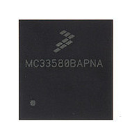
MC33580BAPNA Freescale, MC33580BAPNA Datasheet - Page 16

MC33580BAPNA
Manufacturer Part Number
MC33580BAPNA
Description
Manufacturer
Freescale
Datasheet
1.MC33580BAPNA.pdf
(38 pages)
Specifications of MC33580BAPNA
Switch Type
High Side
Power Switch Family
MC33580
Input Voltage
6 to 27V
Power Switch On Resistance
30mOhm
Number Of Outputs
4
Mounting
Surface Mount
Supply Current
20mA
Package Type
Power QFN
Operating Temperature (min)
-40C
Operating Temperature Classification
Automotive
Pin Count
24
Lead Free Status / RoHS Status
Compliant
Available stocks
Company
Part Number
Manufacturer
Quantity
Price
voltage automotive and industrial lighting and motor control
applications. Its four low R
control the high sides of four separate resistive or inductive
loads.
using a 16-bit SPI interface. Additionally, each output has its
own parallel input for PWM control if desired. The 33580
OUTPUT CURRENT MONITORING (CSNS)
the designated HS0 : HS3 output. That current is fed into a
ground-referenced resistor and its voltage is monitored by an
MCU's A/D. The output to be monitored is selected via the
SPI. This pin can be tri-stated through SPI.
SERIAL INPUTS (IN0, IN1, IN2, IN3)
control HS0 : HS3 high-side output pins, respectively. An SPI
register determines if each input is activated or if the input
logic state is OR ed or AND ed with the SPI instruction. These
pins are to be driven with 5.0 V CMOS levels, and they have
an active internal pulldown current source.
TEMPERATURE FEEDBACK (TEMP)
temperature of the GND. It is used by the MCU to monitor
board temperature.
FAULT STATUS (FS)
external pullup resistor to V
fault condition is detected, this pin is active LOW. Specific
device diagnostic faults are reported via the SPI SO pin.
WAKE (WAKE)
timeout feature if enabled. An internal clamp protects this pin
from high damaging voltages when the output is current
limited with an external resistor. This input has a passive
internal pulldown.
RESET (RST)
and fault registers, as well as place the device in a low-
current sleep mode. The pin also starts the watchdog timer
when transitioning from logic [0] to logic [1]. This pin should
not be allowed to be logic [1] until V
pin has a passive internal pulldown.
16
33580
FUNCTIONAL DESCRIPTION
INTRODUCTION
The 33580 is one in a family of devices designed for low-
Programming, control, and diagnostics are accomplished
The Current Sense pin sources a current proportional to
The IN0 : IN3 high-side input pins are used to directly
This pin reports an analog voltage value proportional to the
This pin is an open drain configured output requiring an
This input pin controls the device mode and watchdog
This input pin is used to initialize the device configuration
DS(ON)
DD
for fault reporting. If a device
MOSFETs (15 mΩ) can
DD
is in regulation. This
FUNCTIONAL DESCRIPTION
FUNCTIONAL PIN DESCRIPTION
INTRODUCTION
allows the user to program via the SPI the fault current trip
levels and duration of acceptable lamp inrush or motor stall
intervals. Such programmability allows tight control of fault
currents and can protect wiring harnesses and circuit boards
as well as loads.
nonleaded PQFN package with exposed tabs.
CHIP SELECT (CS)
microcontroller (MCU). When this pin is in a logic [0] state,
the device is capable of transferring information to, and
receiving information from, the MCU. The 33580 latches in
data from the Input Shift registers to the addressed registers
on the rising edge of
information from the power output to the Shift register on the
falling edge of
is logic [0].
state only when SCLK is a logic [0].
pullup, I
SERIAL CLOCK (SCLK)
33580 device. The serial input (SI) pin accepts data into the
input shift register on the falling edge of the SCLK signal
while the serial output (SO) pin shifts data information out of
the SO line driver on the rising edge of the SCLK signal. It is
important the SCLK pin be in a logic low state whenever
makes any transition. For this reason, it is recommended the
SCLK pin be in a logic [0] whenever the device is not
accessed (
pulldown. When
pins are ignored and SO is tri-stated (high impedance) (see
Figure
SERIAL INPUT (SI)
Each SI bit is read on the falling edge of SCLK. A 16-bit
stream of serial data is required on the SI pin, starting with
D15 to D0. The internal registers of the 33580 are configured
and controlled using a 5-bit addressing scheme described in
Table
described in
internal pulldown, I
DIGITAL DRAIN VOLTAGE (VDD)
power to the SPI circuit. In the event V
The 33580 is packaged in a power-enhanced 12 x 12
The
The SCLK pin clocks the internal shift registers of the
This is a serial interface (SI) command data input pin.
This pin is an external voltage input pin used to supply
8, page 22. Register addressing and configuration are
9, page 18).
CS
UP
.
pin enables communication with the master
CS
CS
Table
CS
logic [1] state). SCLK has an active internal
should transition from a logic [1] to a logic [0]
CS
. The SO output driver is enabled when
DWN
9, page 22. The SI input has an active
is logic [1], signals at the SCLK and SI
CS
Analog Integrated Circuit Device Data
.
. The device transfers status
Freescale Semiconductor
CS
DD
has an active internal
is lost, an internal
CS
CS


