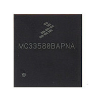
MC33580BAPNA Freescale, MC33580BAPNA Datasheet - Page 24

MC33580BAPNA
Manufacturer Part Number
MC33580BAPNA
Description
Manufacturer
Freescale
Datasheet
1.MC33580BAPNA.pdf
(38 pages)
Specifications of MC33580BAPNA
Switch Type
High Side
Power Switch Family
MC33580
Input Voltage
6 to 27V
Power Switch On Resistance
30mOhm
Number Of Outputs
4
Mounting
Surface Mount
Supply Current
20mA
Package Type
Power QFN
Operating Temperature (min)
-40C
Operating Temperature Classification
Automotive
Pin Count
24
Lead Free Status / RoHS Status
Compliant
Available stocks
Company
Part Number
Manufacturer
Quantity
Price
one of three overcurrent fault blanking times defined in
Table
overcurrent low detection levels. If the selected overcurrent
high level is reached, the device will latch off within 20 µs
Table 13. Overcurrent Low Detection Blanking Time
low detection feature. When disabled, there is no timeout for
the selected output and the overcurrent low detection feature
is disabled.
(OL) detection feature for the output corresponding to the
state of bits D12 : D11.
ADDRESS A
REGISTER (DICR)
or configure the direct IN pin control of each output. Each
output is independently selected for configuration based on
the state bits D12 : D11 (refer to
will enable the output for direct control. A logic [1] on bit D1
will disable the output from direct control.
direct control, a logic [1] for the D0 (A/O_s) bit will result in a
Boolean AND of the IN pin with its corresponding IN_SPI
D[4:0] message bit when addressing OCR0. Similarly, a logic
[0] on the D0 pin results in a Boolean OR of the IN pin to the
corresponding message bits when addressing the OCR0.
This register is especially useful if several loads are required
to be independently PWM controlled. For example, the IN
pins of several devices can be configured to operate all of the
outputs with one PWM output from the MCU. If each output
is then configured to be Boolean ANDed to its respective IN
pin, each output can be individually turned OFF by SPI while
controlling all of the outputs, commanded on with the single
PWM output.
high ratio on the CSNS pin for the selected output. The
default value [0] is used to select the low ratio
24
33580
FUNCTIONAL DEVICE OPERATION
LOGIC COMMANDS AND REGISTERS
*
“_s” refers to the output, which is selected through bits D12
Bits D1 : D0 (OCLT1_s : OCLT0_s) allow the MCU to select
A logic [1] on bit D2 (OCL_DIS_s) disables the overcurrent
A logic [1] on bit D3 (OL_DIS_s) disables the open load
The DICR register is used by the MCU to enable, disable,
For the selected output, a logic [0] on bit D1 (DIR_DIS_s)
While addressing this register, if the Input was enabled for
A logic [1] on bit D2 (CSNS_high_s) is used to select the
13. Note that these time-outs apply only to the
OCLT[1:0]_s
00
01
10
11
1
A
0
100 — DIRECT INPUT CONTROL
*
Table
10, page 23).
Do not use
Timing
155 ms
150 µs
75 ms
(Table
14).
:
D11.
.
high speed slew rate for the selected output, the default value
[0] corresponds to the low speed slew rate.
ADDRESS 00101 — UNDERVOLTAGE /
OVERTEMPERATURE REGISTER (UOVR)
overvoltage (D0) protection. When these two bits are [0], the
under- and overvoltage are active (default value).
latching on the HS0 and HS1. To latch the overtemperature,
the bits (OT_latch_1 and OT_latch_0) must be set to [0]
which is the default value. To disable the latching, both bits
must be set to [1].
ADDRESS 01101 — WATCHDOG AND HS[2,3]
OVERTEMPERATURE REGISTER (WDR)
Watchdog timeout. The Watchdog timeout is configured
using bits D1 and D0. When D1 and D0 bits are programmed
for the desired watchdog timeout period
WDSPI bit should be toggled as well, ensuring the new
timeout period is programmed at the beginning of a new
count sequence.
latching on the HS2 and HS3. To latch the overtemperature,
the bits (OT_latch_3 and OT_latch_2) must be set to [0]
which is the default value. To disable the latching, both bits
must be set to [1].
OVERVOLTAGE AND HS[0,1]
Table 14. Current Sense Ratio
Table 15. Watchdog Timeout
*
refer to
“_s” refers to the output, which is selected through bits D12
A logic [1] on bit D3 (FAST_SR_s) is used to select the
The UOVR register disables the undervoltage (D1) and/or
The UOVR register allows the overtemperature detection
The WDR register is used by the MCU to configure the
The WDR register allows the overtemperature detection
CSNS_high_s
WD[1:0] (D1, D0)
Table
10, page 23.
00
01
10
11
0
1
*
(D2)
Analog Integrated Circuit Device Data
Freescale Semiconductor
Current Sense Ratio
Timing (ms)
HS0 to HS3
(Table
1/13000
1/38000
2250
1125
558
279
15), the
:
D11;


